Phase-Noise Modeling, Simulation, and Propagation in Phase-Locked Loops (Part 2)
What you’ll learn:
- Some brief theory and typical measurements of phase noise.
- Standard analysis of PLL phase noise used by most CAD applications.
- How to produce the lowest phase noise at a PLL output.
- A standard design procedure for a typical Type 2, second-order loop.
As noted in Part 1, phase-locked loops (PLLs) are ubiquitous in today’s high-tech world. Almost all commercial and military products employ them in their operation and phase (or PM) noise is a major concern. Frequency (or FM) noise is closely related (instantaneous frequency is the time derivative of phase) and is generally considered under the umbrella of phase noise (perhaps both might be considered “angle noise”). Amplitude (or AM) noise is another consideration.
While both affect PLL performance, amplitude noise is usually self-limiting and of no consequence. Phase noise, therefore, at the PLL output and of the RF components, is the dominant concern. Of course, output phase noise is the ultimate concern and depends critically on the phase noise of each component. A number of factors contribute to component phase noise, such as power supplies, EMI and semiconductor anomalies, to name a few, and understanding these factors allows us to implement mitigation strategies for component phase noise and, ultimately, output phase noise.
Part 1 discussed brief theory and typical measurements of phase noise along with the analysis (modeling, simulation, and propagation) thereof, and showed the method used by most computer-aided-design (CAD) applications. Part 2 digs into the design of a hypothetical PLL frequency synthesizer to be used for analysis.
Design of 8- to 12-GHz Output/50-MHz Step PLL Frequency Synthesizer
To demonstrate the concepts and methods reviewed in Part 1, we design a hypothetical single loop 8- to 12-GHz/50-MHz step (channel spacing) integer synthesizer with a 25-MHz reference (50 MHz being the smallest achievable step since, looking ahead, we will use a fixed modulus divide-by-2 prescaler). It will be designed for the lowest average output phase noise across the band by achieving the lowest phase noise at the 10-GHz mid-band output. We follow a standard design procedure:
1. Review specifications.
For this example, the sole specification is phase noise (an impractical oversimplification explicitly for this example) as described above.
2. Select circuit configuration, type, order, and loop-filter topology.
Discrete (rather than IC or hybrid) configuration, Type 2, second-order with first-order active PI loop filter (chosen because of its simplicity and popularity).
3. Select components.
Reference: Prominent electronics manufacturer’s 100-MHz OCVCXO (Figs. 5 and 6).
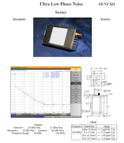
5. Reference (100-MHz OCVCXO) datasheet from manufacturer for 8- to 12-GHz output/50-MHz step PLL frequency synthesizer.

6. Reference (100-MHz OCVCXO) phase-noise plot (Fig. 5) with General Phase Noise Model (Fig. 3 from Part 1) fit to plot for 8- to 12-GHz output/50-MHz step PLL frequency synthesizer.
Reference Divider: Prominent electronics manufacturer’s Programmable Integer Divider with range Kr (= 1/R) = 1/1 to 1/17 (R = 1 to 17) programmed to:
R = 4 at All GHz
Feedback Divider: Prominent electronics manufacturer’s programmable integer/fractional divider used in integer mode with range Km (= 1/M) = 1/32 to 1/1048575 (M = 32 to 1048575) programmed to:
M = 160 at 8 GHz
M = 180 at 9 GHz
M = 200 at 10 GHz
M = 220 at 11 GHz
M = 240 at 12 GHz
Prescaler: Prominent electronics manufacturer’s fixed modulus divide-by-2 prescaler with Kp (= 1/P) = 1/2 (P = 2) giving total feedback factor of Kn (=1/N) = 1/MP (N=MP) producing:
P = 2 at All GHz
N = MP = 320 at 8 GHz
N = MP = 360 at 9 GHz
N = MP = 400 at 10 GHz
N = MP = 440 at 11 GHz
N = MP = 480 at 12 GHz
VCO: Prominent electronics manufacturer’s 8- to 12.5-GHz low-noise VCO11 with:
Kv = 900 MHz/V [5.7(109) rad/S/V] at 8 GHz
Kv = 825 MHz/V [5.2(109) rad/S/V] at 9 GHz
Kv = 725 MHz/V [4.6(109) rad/S/V] at 10 GHz
Kv = 540 MHz/V [3.4(109) rad/S/V] at 11 GHz
Kv = 375 MHz/V [2.4(109) rad/S/V] at 12 GHz
Phase Detector: Prominent electronics manufacturer’s phase/frequency detector (PFD) with gain-control circuit to compensate for Kv variations across the VCO band (maintaining KϕKv = constant) to produce effective:
Kϕ = 0.134 V/rad at 8 GHz
Kϕ = 0.147 V/rad at 9 GHz
Kϕ = 0.166 V/rad at 10 GHz
Kϕ = 0.225 V/rad at 11 GHz
Kϕ = 0.318 V/rad at 12 GHz
Loop filter/Error amplifier: Prominent electronics manufacturer’s op amp (with adequate gain, precision, noise, bandwidth, stability, power-supply requirements, and output-voltage/current-drive capabilities).
4. Develop phase-noise models for the RF components.
We use steps 1 to 6 of our Phase Noise Analysis Procedure (from Part 1) to develop the RF component phase-noise models and simulate them in Figure 7. We show the complete development for the Reference including the General Phase Noise Model (Fig. 3, Part 1) fitted to its datasheet phase-noise plot (Figs. 5 and 6) along with its calculations and resulting specific phase-noise model.
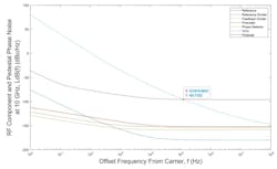
7. RF component and pedestal phase noise at 10-GHz mid-band output showing optimal loop bandwidth, fg, at VCO/pedestal intersection for 8- to 12-GHz output/50-MHz step PLL frequency synthesizer.
For the other components, we only show their calculations and resulting specific phase-noise models for brevity (also, for simplicity, the loop filter/error amplifier isn’t modeled since it’s not an RF component and its analysis is more complex than that for an RF component1):
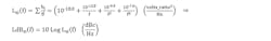
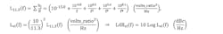
A. Reference (at 100 MHz)
Phase-noise model points, LdBj(fk), from fitting General Phase Noise Model to datasheet plot:
Floor Segment: 0 dB/dec (17 kHz - ∞ Hz)
Floor-point: LdB0(fa) = −180(17 kHz) (dBc/Hz)
L0(fa) = 10LdB0/10 = 10-18.0(17 kHz) (volts_ratio2/Hz)
Flicker Segment: −10 dB/dec (7 kHz - 17 kHz)
Mid-point: LdB1(fb) = −178(11 kHz) (dBc/Hz)
L1(fb) = 10LdB1/10 = 10-17.8(11 kHz) (volts_ratio2/Hz)
Flicker Segment: −20 dB/dec (200 Hz - 7 kHz)
Mid-point: LdB2(fc) = −159(1 kHz) (dBc/Hz)
L2(fc) = 10LdB2/10 = 10-15.9(1 kHz) (volts_ratio2/Hz)
Flicker Segment: −30 dB/dec (10 Hz - 200 Hz)
Mid-point: LdB3(fd) = −127(50 Hz) (dBc/Hz)
L3(fd) = 10LdB3/10 = 10-12.7(50 Hz) (volts_ratio2/Hz)
Phase-noise model coefficients, hj, from above phase-noise model points:
h0 = L0fa0 = 10-18.0 (volts_ratio2Hz-1)
h1 = L1fb1 = (10-17.8)[11(103)]1 = 10-13.8 (volts_ratio2)
h2 = L2fc2 = (10-15.9)(103)2 = 10-9.9 (volts_ratio2Hz)
h3 = L3fd3 = (10-12.7)[5(101)]3 = 10-7.6 (volts_ratio2Hz2)
Phase-noise model, LdBxi(f), from above coefficients:
Simulate LdBxi(f) in Figure 7.
B. Reference Divider (frequency independent)
Phase-noise model points, LdBj(fk), from fitting General Phase Noise Model to datasheet plot (not shown):
Floor Segment: 0 dB/dec (3 kHz - ∞ Hz)
Floor-point: LdB0(fa) = −153(3 kHz) (dBc/Hz)
L0(fa) = 10LdB0/10 = 10-15.3(3 kHz) (volts_ratio2/Hz)
Flicker Segment: −10 dB/dec (100 Hz - 3 kHz)
Mid-point: LdB1(fb) = −150(600 Hz) (dBc/Hz)
L1(fb) = 10LdB1/10 = 10-15.0(600 Hz) (volts_ratio2/Hz)
Phase-noise model coefficients, hj, from above phase-noise model points:
h0 = L0fa0 = 10-15.3 (volts_ratio2Hz-1)
h1 = L1fb1 = (10-15.0)[6(102)]1 = 10-12.2 (volts_ratio2)
Phase-noise model, LdBri(f), from above coefficients:

Simulate LdBri(f) in Figure 7.
C. Feedback Divider (frequency independent)
Phase-noise model points, LdBj(fk), from fitting General Phase Noise Model to data sheet plot (not shown):
Floor Segment: 0 dB/dec (10 kHz - ∞ Hz)
Floor-point: LdB0(fa) = −155(10 kHz) (dBc/Hz)
L0(fa) = 10LdB0/10 = 10-15.5(10 kHz) (volts_ratio2/Hz)
Flicker Segment: -10 dB/dec (100 Hz - 10 kHz)
Mid-point: LdB1(fb) = −143(1 kHz) (dBc/Hz)
L1(fb) = 10LdB1/10 = 10-14.3(1 kHz) (volts_ratio2/Hz)
Phase-noise model coefficients, hj, from above phase-noise model points:
h0 = L0fa0 = 10-15.5 (volts_ratio2Hz-1)
h1 = L1fb1 = (10-14.3)(103)1 = 10-11.3 (volts_ratio2)
Phase-noise model, LdBfi(f), from above coefficients:

Simulate LdBfi(f) in Figure 7.
D. Prescaler (frequency independent)
Phase-noise model points, LdBj(fk), from fitting General Phase Noise Model to datasheet plot (not shown):
Floor Segment: 0 dB/dec (10 kHz - ∞ Hz)
Floor-point: LdB0(fa) = −152(10 kHz) (dBc/Hz)
L0(fa) = 10LdB0/10 = 10-15.2(10 kHz) (volts_ratio2/Hz)
Flicker Segment: −10 dB/dec (100 Hz - 10 kHz)
Mid-point: LdB1(fb) = −142(1 kHz) (dBc/Hz)
L1(fb) = 10LdB1/10 = 10-14.2(1 kHz) (volts_ratio2/Hz)
Phase-noise model coefficients, hj, from above phase-noise model points:
h0 = L0fa0 = 10-15.2 (volts_ratio2Hz-1)
h1 = L1fb1 = (10-14.2)(103)1 = 10-11.2 (volts_ratio2)
Phase-noise model, LdBpi(f), from above coefficients:

Simulate LdBpi(f) in Figure 7.
E. VCO (at 10 GHz scaled from 11.3 GHz given on datasheet)
Phase-noise model points, LdBj(fk), from fitting General Phase Noise Model to datasheet plot at 11.3 GHz (not shown):
Floor Segment: 0 dB/dec (100 MHz - ∞ Hz)
Floor-point: LdB0(fa) = −150(100 MHz) (dBc/Hz)
L0(fa) = 10LdB0/10 = 10-15.0(100 MHz) (volts_ratio2/Hz)
Flicker Segment: -10 dB/dec (10 MHz - 100 MHz)
Mid-point: LdB1(fb) = −143(30 MHz) (dBc/Hz)
L1(fb) = 10LdB1/10 = 10-14.3(30 MHz) (volts_ratio2/Hz)
Flicker Segment: −20 dB/dec (40 kHz - 10 MHz)
Mid-point: LdB2(fc) = −111(600 kHz) (dBc/Hz)
L2(fc) = 10LdB2/10 = 10-11.1(600 kHz) (volts_ratio2/Hz)
Flicker Segment: −30 dB/dec (1 kHz - 40 KHz)
Mid-point: LdB3(fd) = −59(6 kHz) (dBc/Hz)
L3(fd) = 10LdB3/10 = 10-5.9(6 kHz) (volts_ratio2/Hz)
Flicker Segment: −40 dB/dec (100 Hz - 1 kHz)
Mid-point: LdB4(fe) = −18(300 Hz) (dBc/Hz)
L4(fe) = 10LdB4/10 = 10-1.8(300 kHz) (volts_ratio2/Hz)
Phase-noise model coefficients, hj, from above phase-noise model points at 11.3 GHz:
h0 = L0fa0 = 10-15.0 (volts_ratio2Hz-1)
h1 = L1fb1 = (10-14.3)[3(107)]1 = 10-6.8 (volts_ratio2)
h2 = L2fc2 = (10-11.1)[6(105)]2 = 100.5 (volts_ratio2Hz)
h3 = L3fd3 = (10-5.9)[6(103)]3 = 105.4 (volts_ratio2Hz2)
h4 = L4fe4 = (10-1.8)[3(102)]4 = 108.1 (volts_ratio2Hz3)
Phase-noise model, LdBvi(f), from above coefficients [L11.3(f) at 11.3 GHz given on datasheet scaled to Lvi(f) at 10 GHz]:
Simulate LdBvi(f) in Figure 7.
F. Phase Detector (at 25 MHz)
Phase-noise model points, LdBj(fk), from fitting General Phase Noise Model to datasheet plot (not shown):
Floor Segment: 0 dB/dec (1 kHz - ∞ Hz)
Floor-point: LdB0(fa) = −159(1 kHz) (dBc/Hz)
L0(fa) = 10LdB0/10 = 10-15.9(1 kHz) (volts_ratio2/Hz)
Flicker Segment: −10 dB/dec (100 Hz - 1 kHz)
Mid-point: LdB1(fb) = −154(300 Hz) (dBc/Hz)
L1(fb) = 10LdB1/10 = 10-15.4(300 kHz) (volts_ratio2/Hz)
Phase-noise model coefficients, hj, from above phase-noise model points:
h0 = L0fa0 = 10-15.9 (volts_ratio2Hz-1)
h1 = L1fb1 = (10-15.4)[3(102)]1 = 10-12.9 (volts_ratio2)
Phase-noise model, LdBdi(f), from above coefficients:

Simulate LdBdi(f) in Figure 7.
G. Loop Filter/Error Amplifier (frequency N/A)
Not modeled, as mentioned, since it’s not an RF component with intrinsic phase noise. Modeling its effective phase noise, as well as calculating its propagation dynamics that contribute to output phase noise, is more complex than for an RF component.1
5. Determine the loop bandwidth, fg, from the sole specification of the lowest average output phase noise across the band by achieving the lowest phase noise at the 10-GHz mid-band output.
The loop optimum bandwidth, fg, is determined from the intersection of the VCO and pedestal (see definition below) phase-noise curves at the 10-GHz mid-band output.
VCO phase-noise model at 10 GHz, LdBvi(f), and curve is as is in the aforementioned section 4, part E.
Pedestal phase noise model at 10 GHz, LdBpl(f), and curve, where the pedestal is defined as the sum of all RF components’ (except the VCO) phase-noise models, Lsi(f), multiplied by the output transfer function’s (to be discussed later) dc gain squared, N2:
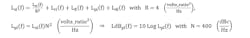
Simulate LdBpl(f) in Figure 7.
The loop bandwidth is then determined either mathematically or graphically and is found to be fg = 121.6 kHz.
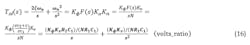
6. Determine the standard parameters fn and ζ.
We determine fn by using rule-of-thumb fn = fg / 1.55 for ζ = 0.707 (Reference 2) and we determine ζ from other specifications (other specifications not given so ζ = 0.707 is retained as default). These were found to be:
fn = 78.5 kHz
ζ = 0.707
7. Equate the open-loop transfer function, Tol, 2nd order form (bold) to the circuit constant form (bold), which gives standard parameters fn and ζ in terms of circuit constants R1, R2, and C1.
(convert to ωn = 2πfn)
which gives the desired relations (bold):
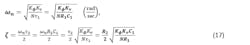
8. Determine circuit constants R1, R2, and C1 (bold) as functions of standard parameters fn and ζ for the 10-GHz mid-band output (N = 400) and calculate any other quantities of interest; modify theoretical values to closest EIA 5% standard values.
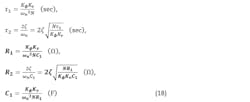
(convert back to fn = ωn/2π).
Note that R1, R2, and C1 are not uniquely determined, so an absolute selection must be made for one of them, usually C1. For this case, select C1, then calculate R1 and R2 (all for resonant frequency of fn = 78.5 kHz and damping factor of ζ = 0.707), where C1 is selected to keep R1 and R2 relatively low. Therefore, resistive noise is insignificant relative to error amplifier (op amp) noise, and within practical limits:12,13
C1 = 0.015 µF (already 5% standard value)
R1 = 522.9 Ω (5% standard value is 510 Ω)
R2 = 191.1 Ω (5% standard value is 200 Ω)
Using these standard values, the design is done and the system is configured by applying the General PLL Block Diagram and Phase Noise Propagation Model (Fig. 4, Part 1) to our specific case to form the Specific PLL Block Diagram & Phase Noise Propagation Model at 10 GHz Mid-band Output for Example PLL (Fig. 8).14

8. Specific PLL Block Diagram & Phase Noise Propagation Model at 10-GHz mid-band output for 8- to 12-GHz output/50-MHz step PLL frequency synthesizer.
9. Model PLL open-/closed-loop dynamics and output phase noise, and simulate performance using appropriate modeling/simulation tool.
Adjust model theoretical (standard value) circuit constants and open-loop gain as needed for closest agreement between simulated and calculated loop dynamics, as well as output phase noise due to discrepancies between calculated and simulated performance.
10. Build and test EDM unit.
Using adjusted circuit constants, build and test the EDM unit. Further adjust EDM circuit constants as needed for proper performance due to discrepancies between simulated and EDM performance.
11. Adjust model open-loop gain as needed for agreement between the model and EDM unit.
So, the design is complete using the theoretical (standard value) circuit constants as determined in step 8. These values would then be refined according to steps 9, 10, and 11, but since we’re not building an EDM for our example, the theoretical values complete the design.
The above information will be used in the final Part 3, where we analyze our example hypothetical synthesizer to demonstrate the concepts and methods presented.
References
1. F. M. Gardner, "Phaselock Techniques", 3rd ed., John Wiley, Hoboken, NJ, 2005.
2. R. E. Best, "Phase-Locked Loops, Design, Simulation and Applications", 6th ed., McGraw-Hill, New York, NY, 2007.
3. P. V. Brennan, "Phase-Locked Loops: Principles and Practice", McGraw-Hill, New York, NY, 1996.
4. E. Drucker, "Phase Lock Loops and Frequency Synthesis for Wireless Engineers", 1997, Frequency Synthesis & Phase-Locked Loop Design, 3 Day Short Course, Besser Associates, Mountain View, CA, 1999.
5. F. C. Weist, "Phase Locked Loop Basics for Frequency Synthesizer Applications", Short Course, Clarksburg, MD, 2011.
6. P. Z. Peebles, Jr., "Probability, Random Variables and Random Signal Principles"', McGraw-Hill, New York, NY, 1980.
7. A. Godone, S. Micalizio and F. Levi, "RF spectrum of a carrier with a random phase modulation of arbitrary slope", Istituto Nazionale di Ricerca Metrologic, INRIM, Strada delle Cacce 91, 10135 Torino, Italy, Metrologia, vol. 45, pp. 313-324, BIPM and IOP Publishing Ltd., Bristol BS1 6HG, UK, May 2008.
8. B. Nelson, "Phase noise 101: basics, applications and measurements", Keysight Technologies, 2018.
9. A. El Gamal, EE278 Lecture Notes 7: "Stationary random processes", Dept. of Electrical Engineering, College of Engineering, Stanford University, Stanford, CA, Autumn 2015.
10. K. J. Button, ed., Infrared and Millimeter Waves, Volume 11: Millimeter Components and Techniques, Part III, Chapter 7: "Phase Noise and AM Noise Measurements in the Frequency Domain", A. L. Lance, W. D. Seal and F. Labaar, TRW Operations and Support Group, One Space Park, Redondo Beach, CA, Academic Press, Cambridge, MA, 1984.
11. Harney, A., "Designing high-performance phase-locked loops with high-voltage VCOs", Analog Dialogue, pp. 43-12, December 2009.
12. "Op amps for everyone", Design Reference, Literature Number SLOD006A, Texas Instruments Inc., Dallas, Texas, 2001.
13. "Noise analysis in operational amplifier circuits", Application Report, Literature Number SLVA043B, Texas Instruments Inc., Dallas, Texas, 2007.
14. Motorola Communications Device Data, Data Book, DL136/D, REV 4, Phoenix, AZ, 1995.
About the Author
Frederick Weist
Principal, FCW Sciences
Frederick Weist presently resides in Point of Rocks, Md. He was born in Phila., Pa., on March 25, 1959. He obtained his BS in physics from Drexel University in 1983 and his MS in physics from the same institution in 1992.
Mr. Weist is presently retired, but continues his interest in research and writing by working as Principal at FCW Sciences. His last position was as Principal Engineer/SME with Boeing Co. - Digital Receiver Technology Subsidiary, Germantown, Md. Previously he held positions as Senior Design Engineer with Kratos Defense and Security Solutions - Herley-CTI Division; Principal Engineer with DRS Technologies - Signal Solutions Division; Senior Engineer with Aydin Corp. - Telemetry Division; and Electronics Engineer with the U.S. Naval Air Warfare Center - Aircraft Division (NAWCAD).
His previous interests included research, design and development of systems from dc to 42 GHz, specializing in PLLs, frequency synthesizers, transceivers, subsystems, and components. He’s also worked in the fields of photonics, magnetics, superconductivity, sensors, and servo systems. Present interests include the same as well as integrated microwave/photonics, quantum, and biophysics systems.
Mr. Weist is a member of the American Physical Society and the Institute of Electrical and Electronics Engineers.
