How Edge Processing Enables Next-Gen mmWave Scanners

Members can download this article in PDF format.
What you'll learn:
- Basic operation of mmWave imaging.
- Key components of mmWave imaging: transmitter, receiver, multichannel ADC.
- How to build a setup for security scanning systems and similar applications.
Millimeter-wave (mmWave) imaging has become an important part of security scanning systems in airports, public buildings, and stadia. Millimeter-wave scanners are superior to traditional metal detectors because they can identify and locate both metallic and nonmetallic threats. This article dives into the specifics of mmWave imaging hardware and looks at a chipset that uses edge processing to manage massive data loads, which is essential in the development of walkthrough security scanning systems.
How Does mmWave Imaging Work?
Figure 1 illustrates the operation of a mmWave scanner. The system consists of an array of transmitters and receivers connected to a spatially dispersed antenna array. It’s analogous to a network analyzer that measures return loss or S11.
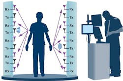
At any time, one antenna in the array transmits a low-power signal at a single frequency. This signal reflects off the target and generates backscatter (the illustration shows reflection from a single point on the target but in practice the transmitted signal is omnidirectional, so there will be reflections from multiple points on the target).
The phase and amplitude of the backscatter are measured by all of the receive antennas in the array. Polarization may be used between the transmit and receive antennas to reduce direct transmit-to-receive leakage. Once this measurement is complete, the same signal is transmitted from another transmit antenna (operating at the same frequency) and the measurement process is repeated.
Because the depth of penetration of RF signals and the nature of the reflection vary with frequency, the scan described earlier is typically repeated at multiple frequencies, across a wide band. The resulting matrix of vectors forms a multidimensional array (vs. frequency and spatial location) that’s used to create an image which can identify metallic and nonmetallic objects concealed between and under layers of clothing.
The hardware required to complete such a scan must be multichannel and have a wide operating frequency range. The 10- to 40-GHz frequency range is wide enough to differentiate the objects in a typical security scanning scenario (clothing, backpacks, weapons, and explosives).
Higher channel count systems tend to have higher resolution, giving them the ability to identify small objects. For example, while detecting a razor blade is critical in airport scanners, securing public buildings and stadia focuses more on the detection of larger items, such as weapons or explosives. In these applications, a lower channel count is typically used.
Another critical component in these systems is fast switching time. This enables the realization of scanning systems where the person being scanned need only pose for a short amount of time (typically one second or less). Next-generation walkthrough systems require faster switching times so that the person doesn’t have to stop and pose.
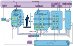
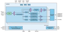
Figure 2 shows how a mmWave imaging chipset from Analog Devices can be used to implement a complete mmWave scanner. An array of transmitters (ADAR2001) is driven from a central agile frequency source. An array of receivers (ADAR2004) detects the reflected signals and downconverts them to a low intermediate frequency, at which they’re IF sampled by a multichannel continuous-time sigma-delta (CTSD) converter (AD9083).
Let’s now take a closer look at these components and how their functionality optimizes overall system performance.
Transmitter for mmWave Imaging Setup
As already noted, the transmitter consists of a large channel count of spatially dispersed antennas, each driven by a power amplifier. The ADAR2001 is a four-channel transmitter that connects directly to the antennas and has an output frequency range of 10 to 40 GHz. Because of the difficulty associated with distributing a 10- to 40-GHz signal in a large array, the ADAR2001 incorporates a 4× multiplier. As a result, all of the plumbing and signal distribution in front of the transmitter ICs happens in the 2.5- to 10-GHz frequency range.
The main RF elements of the ADAR2001 transmitter are an RF input buffer, a 4× frequency multiplier with integrated switchable harmonic filters, a 1:4 signal splitter, and four differential-out power amplifiers, which are intended to drive differential antenna structures such as dipole or spiral antennas. Figure 3 shows a detailed block diagram of the ADAR2001.
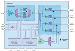
A CW RF input signal between 2.5 and 10 GHz and with a power level of at least –20 dBm is applied to the RFIN port. The broadband frequency multiplier consists of three parallel subcircuits. Each subcircuit (low band, mid band, high band) is optimized to multiply and filter a segment of the total frequency range. Switches at the input and output of the multiplier block are used to select the subcircuit for the desired frequency of operation.
The multiplier output passes through a programmable attenuator (PA) before being split into four and applied to four power amplifiers. In addition to the configurable filtering in the multiplier block, each PA contains a low-pass/notch filter that can be enabled or disabled. For output frequencies up to 20 GHz, this filter should be enabled. Above 20 GHz, it should be disabled.
The PA is used to help ensure relatively flat output power versus frequency. This attenuator has approximately 15 dB of digital step attenuation range. As the output frequency sweeps from 10 to 40 GHz, this attenuation should be decreased to maintain the desired output power flatness versus frequency. This results in a nominal PA output power of +5 dBm on each of the differential PA outputs with harmonic suppression that ranges from –20 to –30 dBc.
To do a complete 10- to 40-GHz frequency sweep, the multiplier/filter block settings must be adjusted seven times to ensure optimum harmonic rejection and output power. In addition, while the system is dwelling at one frequency, each transmitter channel must be successively turned on and off.
To avoid creating a bottleneck of SPI commands, the ADAR2001 includes two state machines that can be preprogrammed with up to 70 states. Once the device’s RAM has been programmed, state advances can be made with a simple pulse to the device’s MADV (advance) pin. These features combine to ensure a 2-ns channel switching time. This switching time is also achievable when switching between ICs (e.g., Channel 4 of Device A is switching off as Channel 1 of Device B is switching on).
Because a full scan involves a full-channel sweep at multiple frequencies, switching time is critical. For example, if the array has 500 elements and is going to sweep from 10 to 40 GHz in 50-MHz steps, it must perform a total of 300,000 channel switches to complete a full scan.
The RF output power on each channel can be monitored using individual, on-chip RF detectors. Die temperature can also be monitored by an on-chip temperature sensor. These sensors feed into a 5:1 analog multiplexer, which passes the desired signal to an on-chip 8-bit ADC.
The ADF4368 PLL/VCO provides the stimulus to the transmitter network. Its output signal will be split multiple times depending on the number of transmit channels. The ADF4368’s relatively high output power of +9 dBm and the minimum input threshold of the ADAR2001 (–20 dBm) ensure that the ADF4368’s output can be passively split many times before amplifier buffering is required.
Receiver for the mmWave Imaging Setup
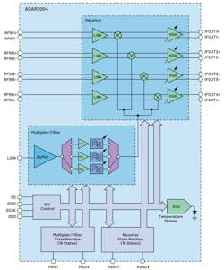
The reflections from the transmission are picked up by the receivers, which are an array of multichannel mixers and ADCs. The ADAR2004 is a quad mixer and ADC driver with a digitally programmed gain amplifier (DGA). The LO input, which also has an internal 4× multiplier, is driven by a second phase-locked loop (PLL) whose output frequency is offset from the radio frequency so that the mixer produces a real IF output. The IF outputs of the mixers are then sampled by the AD9083, a 16-channel CTSD ADC with integrated digital downconversion.
An IF sampling architecture was chosen over a zero-IF architecture to avoid DC offsets that result from LO leakage in the receiver and I/Q errors generated by imperfect quadrature balance in the LO’s quadrature splitter. While these imperfections can be mitigated by calibration, calibration would be required at every input frequency because LO leakage and quadrature errors tend to vary with frequency.
Figure 4 shows a block diagram of the ADAR2004 quad mixer. The LO input is driven by a 2.5- to 10-GHz sine wave that produces 10 to 40 GHz at the output of the multiplier. The multiplier output is fed to the four mixers that have a programmable gain on their IF outputs. Like the ADAR2001 transmitter, the ADAR2004 receiver also has two on-chip state machines that can be preprogrammed.
Multichannel ADC for the mmWave Imaging Setup
Figure 5 illustrates a block diagram of the AD9083, a 16-channel CTSD ADC. The ADC inputs are designed to have the same common-mode voltage as the IF outputs of the ADAR2004. Thus, the mixer output and the ADC input can be connected directly. The absence of AC-coupling capacitors ensures that no charging/discharging transients are present when the mixer output switches abruptly (e.g., during a frequency step at the mixer input).
The use of a first-order CTSD ADC architecture with an integrated single-pole filter saves PCB space by minimizing external filtering. The architecture also enables a fast signal settling time when compared to the settling time of Nyquist-rate converters, which require highly selective antialiasing filters to eliminate noise folding. Fast settling time is a key requirement in this application because the ADC settling time must be able to keep up with the fast channel switching on the transmit side.
Each ADC has a signal-processing tile to filter out-of-band, shaped noise from the sigma-delta ADC and reduce the sample rate. Each tile contains a cascaded-integrator-comb (CIC) filter, a quadrature digital downconverter (DDC) with multiple finite-input-response (FIR) decimation filters (decimate by J block), or up to three quadrature DDC channels with averaging decimation filters for data gating applications. The presence of three quadrature DDC channels enables simultaneous demodulation of up to three frequencies. We’ll see later how this can be used to dramatically speed up the scan time.
System Setup and Operation
The ADAR2001 and ADAR2004 were specifically designed for efficient operation in large arrays. Particular emphasis was placed on reducing wiring overhead. The RFIN and LO input ports of ADAR2001 and ADAR2004 can operate at input levels as low as –20 dBm.
Because it’s desirable to drive these inputs from a common LO source (the ADF4368 in this case), this low input sensitivity allows for lots of passive fanout before amplification is required. For example, if we assume that a Wilkinson power splitter has a net loss of 1 dB, the ADF4368’s output power of 9 dBm can be passively fanned out seven times and can drive 128 devices (512 channels).
The advance and reset pins that drive the ADAR2001 and ADAR2004’s on-chip sequencers are also designed to be driven in parallel to minimize the number of GPIOs that must be provided by the processor or FPGA. By providing enough depth and complexity in the sequencers, it’s possible to drive up to 16 ADAR2001 devices with a single set of advance and reset pulses.
Before operation, the ADAR2001 and ADAR2004’s sequencers must be programmed. While it’s possible to access all of the functionality of both devices using SPI commands, the associated latency would result in an unacceptably long overall scan time.
Let’s consider how to set up a 64-channel system (64-transmitter, 64-receiver) for a channel-based scan. That is, we cycle through all of the transmit channels at a single frequency before incrementing the frequency and repeating the scan.
Figure 6 shows how the state machines in the 16 ADAR2001 devices are programmed to enable this sweep. A key goal of the architecture is to be able to sequence multiple devices that are doing different things from common control lines.

Notice in Figure 6 that while each IC has 65 states, most of the ICs are programmed to be in sleep mode (SLP) the majority of the time. For instance, IC 1 is only fully active for the first four states as channels 1, 2, 3, and 4 of that IC sequentially transmit. During these four states, all other ICs are either in SLP or ready (RDY) mode.
Likewise, IC 2 is only fully active during states 5 to 8, because the other ICs are either in SLP or RDY mode. By configuring the 16 state machines in this manner, with their on cycles offset from one another, it’s possible to drive the advance and reset lines of all 16 devices with parallel pulses.
Ready (RDY) Mode
The RDY mode is an intermediate state of what was developed to optimize switching time while saving power. Because most of the transmitters are inactive most of the time, the SLP mode is key to keeping down power consumption. However, the time required to switch from SLP mode to transmit mode (50 ns) is excessive from a system perspective and would result in delays during the scan.
The RDY mode is an intermediate state that can be invoked when an IC is preparing to transmit. Notice in Figure 6 that in State 4, Channel 4 of IC 1 is transmitting, and IC 2 is being prepared for transmission by placing it in RDY mode. In the transition from transmitter states 4 to 5, IC 1 transitions from transmit mode to RDY mode, and IC 2 transitions from RDY to transmit mode. This transition takes 10 ns. The subsequent on-chip channel switches (i.e., from Channel 1 to Channel 2 to Channel 3 to Channel 4 on IC 2) have a switching time of 2 ns.
For a 1024-element array that sweeps from 10 to 40 GHz in 0.1-GHz steps, the complete scan time would be less than 20 ms. This assumes a PLL lock time of 50 μs. If two PLLs operating in ping-pong mode were used to achieve faster frequency settling, the scan time would be well below 5 ms.
The operation and sequencing of the ADAR2004 receiver are less complex because it’s typical practice to configure all receiver channels to be receiving at all times. The state machines must still be sequenced so that the correct multiplier path and filter settings are chosen as the receiver sweeps in tandem with the transmitter.
As already noted, each AD9083 ADC channel can access up to three quadrature DDC channels. This means that it can simultaneously demodulate three frequencies, assuming that all three frequencies are within the input frequency range of the ADC’s analog input bandwidth (125 MHz). For example, by positioning three IF tones at 50 MHz, 75 MHz, and 100 MHz, all three can be simultaneously demodulated into I and Q baseband data.
To facilitate this approach on the transmit side, three transmit PLLs must be used instead of one. The three transmit frequencies must always be directed to different physical transmit ICs (the multipliers in the ADAR2001 can’t conduct multitone signals). And the three frequencies must always be different but must remain close in frequency to one another as they sweep.
For example, if one channel on one of the ADAR2001 devices is transmitting at 10 GHz, two other devices will be transmitting at 10.025 GHz and 10.050 GHz to support IF outputs at 50, 75, and 100 MHz. This scheme requires more hardware and switching infrastructure in the transmit path, but it has the benefit of reducing the overall scan time by a factor of 3.
Conclusion
The chipset consisting of the ADAR2001 quad transmitter, the ADAR2004 quad receiver, the AD9083 16-channel ADC, and the ADF4368 PLL/VCO provides the means to implement next-generation walkthrough mmWave security scanners. Integrated state machines and on-chip digital downconversion significantly offload traditional centralized processing and move it to the intelligent edge. The net result is that the central processor can worry less about controlling the system during a scan, and the data that it receives is already demodulated and decimated.
While this chipset was developed specifically for mmWave security imaging applications, the wide frequency range of the ADAR2001 transmitter and ADAR2004 receiver, as well as the level of integration of the AD9083 16-channel ADC, make this chipset an option for other applications that require high channel density and fast switching.
About the Author
Eamon Nash
Applications Engineering Director
Eamon Nash is an applications engineering director at Analog Devices. He has worked at ADI in various field and factory roles, covering mixed-signal, precision, and RF products. He’s currently focused on RF amplifiers and beamformer products for satellite communications and radar. He holds a Bachelor of Engineering (B.Eng.) degree in electronics from University of Limerick, Ireland, as well as five patents.
