LDMOS Power Transistors Drive 200 W to 1300 MHz

Download this article in PDF format.
Power transistors for RF/microwave applications exploit a range of different technologies, including substrate materials like the tried-and-true gallium arsenide (GaAs) to the somewhat more recent and intriguing gallium nitride (GaN). Still, silicon transistor substrates remain the longest-running foundations for high-power RF/microwave transistors in both commercial and military applications.
Among those silicon devices, lateral diffused metal-oxide-semiconductor (LDMOS) transistors have demonstrated good reliability with high performance levels. And when new silicon LDMOS power transistors arrive, they provide further options for RF/microwave power-amplifier designers faced with the challenges of trying to optimize performance parameters such as output power, gain, and efficiency over a given bandwidth.
A pair of recently released, +28-V dc silicon LDMOS power transistors from Polyfet RF Devices pack a great deal of punch for power amplifiers through about 1.3 GHz. Models LA2541 and LS2541 are impedance-unmatched silicon LDMOS transistors available in two slightly different push-pull packages. Each transistor is capable of as much as 200 W output power (at 1-dB compression), and versatile enough to drive continuous-wave (CW) or pulsed input waveforms with high efficiency and effective thermal management.
Depending on how they are source and load matched, the two packaged transistors (see figure) can be used in broadband or narrowband applications through 1300 MHz and deliver high output power with high gain and efficiency. Each device employs back-to-back gate diodes for enhanced electrostatic-discharge (ESD) protection. Their rugged metal-ceramic packages feature clearly marked and easily accessible gate, drain, and source connections to simplify installation into a circuit board for an amplifier designer.
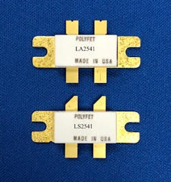
These high-power silicon LDMOS transistors are supplied in a choice of LA (top) and LS (bottom) metal-ceramic flanged packages for ease of use and installation.
Both packages/transistors are rated for total device power dissipation of 460 W, junction-to-case thermal resistance of 0.38ºC/W, maximum dc drain current of 18 A, high maximum drain-to-gate breakdown voltage of 80 V dc, and maximum junction temperature of +200ºC.
In terms of performance, the two transistors offer similar levels. For example, the LA2541 is rated for minimum common source power gain of 16 dB at 500 MHz, when measured at 28 V dc with quiescent drain current (Idq) of 800 mA. It boasts typical drain efficiency of 60% when measured under the same operating conditions at 500 MHz. In addition, it can handle VSWR load mismatches as severe as 20.0:1 at 500 MHz, also under the same operating conditions.
Supplied in its LS package with somewhat modified drain contacts, the LS2541 LDMOS transistor features the same minimum gain, typical drain efficiency, and VSWR load mismatch capabilities when measured at a test frequency of 500 MHz.
Both power transistors are tested and characterized in three different test fixtures, at 500 MHz, 1.3 GHz, and across the frequency range of 30 to 512 MHz. The transistors share electrical characteristics and can be used almost interchangeably in power-amplifier designs, depending on packaging and layout requirements. The packaged transistors incorporate flanges based on copper/copper-molybdenum-copper/copper (Cu/Cu/Mo/Cu or CPC) rather than copper-tungsten (CuW) materials. This enables efficient thermal transfer from transistor die to heat sink and surrounding circuitry for effective heat flow and enhanced device reliability.
Comparing Characteristics
The LA2541 and LS2541 share electrical characteristics, including a gate-source voltage (Vgs) range of 2 to 5 V dc for a drain-source voltage (Vds) at the same setting and a drain-source current (Ids) of 200 mA. The minimum breakdown drain-source voltage (BVdss) is 80 V dc at Ids of 5 mA and Vgs of 0 V dc. The maximum saturated drain-source leakage current (Idss) is 5.0 mA at Vds of 28 V dc and Vgs of 0 V ds. The maximum gate leakage current (Igss) is 1 μA for Vgs of 10 V dc and Vds of 0 V dc. Both packaged power transistors exhibit a typical forward transconductance of 7.5 mhos at Vds of 10 V dc and Vgs of 5 V dc.
Whichever package/transistor is specified, these are high-power RF transistors that can be impedance-matched as needed for narrowband or broadband applications. The simple flanged package styles and use of the latest metal-ceramic packaging materials ensure high reliability and secure mounting capability in any amplifier printed-circuit-board (PCB) design, whether for commercial or military use.
Polyfet RF Devices, 1110 Avenida Acaso, Camarillo, CA 93012; (805) 484-4210, E-mail: [email protected].

About the Author
Jack Browne
Technical Contributor
Jack Browne, Technical Contributor, has worked in technical publishing for over 30 years. He managed the content and production of three technical journals while at the American Institute of Physics, including Medical Physics and the Journal of Vacuum Science & Technology. He has been a Publisher and Editor for Penton Media, started the firm’s Wireless Symposium & Exhibition trade show in 1993, and currently serves as Technical Contributor for that company's Microwaves & RF magazine. Browne, who holds a BS in Mathematics from City College of New York and BA degrees in English and Philosophy from Fordham University, is a member of the IEEE.
