CVD Diamond Manages Device Heat Effectively
Download the PDF of this article.
Heat can be damaging to the semiconductor devices that produce it, unless it is allowed to flow away from those devices. Solid-state devices such as GaN transistors continue to advance in terms of increased power densities at higher operating frequencies, but they also generate large amounts of heat in small areas, and their performance levels and reliability will be limited by how quickly and completely the heat can be dissipated. Quite simply, higher-power levels are possible with a large-signal semiconductor when the right heat-spreader material is used. In terms of thermal management, diamond is that optimum heat-spreading material, offering thermal conductivities up to 10× those of other commonly used heat-spreading ceramics.
Commercial GaN transistors and integrated circuits (ICs) have been fabricated on various heat-spreading base substrates, such as silicon (Si) and silicon carbide (SiC), with fair results in terms of thermal management. Still, the heat spreading capabilities of these materials can put a ceiling on the maximum output power that can be achieved from a GaN-based solid-state device. The thermal conductivity of SiC, at 400 W/m-K, has been considered suitable for dissipating heat from GaN devices. Single devices capable of high power levels at RF/microwave frequencies have been developed on GaN-on-SiC processes for commercial, industrial, and military applications.
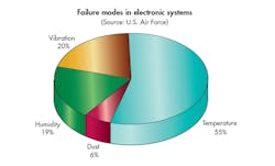
Modern electronic systems often fail due to lack of adequate thermal management (Fig. 1). The choice of materials for a thermal management design and the methodology of the application are essential to minimizing channel temperatures and ensuring reliable long-term device operation. Until now, GaN-on-SiC devices have demonstrated the most effective management of heat in high-power discrete transistors and monolithic-microwave-integrated-circuit (MMIC) components. Still, the heat-spreading capabilities of SiC are limited and typically the maximum power dissipation of GaN-on-SiC devices is derated to protect long-term reliability. To achieve higher power levels with less heat, especially for circuits with densely packed active (heat-generating) GaN devices, chemical vapor deposition (CVD) diamond enables much higher power densities than conventional approaches.
1. Of the causes of failure in electronic systems, heat is the most damaging.
Diamond is a versatile material for many industries, with excellent mechanical and electrical characteristics. It has many useful properties for electrical applications, including the highest known thermal conductivity,1 stiffness, and hardness, combined with high optical transmission across a wide wavelength range, low expansion coefficient, and low density. These exceptional characteristics can make diamond the ultimate solution for thermal management problems.
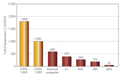
To synthesize diamond for this purpose, the first step is choosing the most suitable deposition technology. Microwave-assisted CVD enables the best control of grain size and grain interfaces for producing high-quality, high-repeatability, polycrystalline diamond with the thermal conductivity needed for particular applications. CVD diamond is now commercially available in different grades with thermal conductivities between 1,000 and 2,000 W/m-K. CVD diamond has fully isotropic characteristics, so that heat will spread in all directions. Figure 2 shows a comparison of CVD diamond with other materials traditionally used for heat spreading purposes.
2. Shown is a comparison of CVD diamond with “traditional” heat-spreading materials.
To harvest the maximum heat-spreading effectiveness of diamond for semiconductor device applications such as GaN semiconductors, both package integration issues and functional requirements must be considered. Since the surfaces of electronic components are typically very smooth and flat, an effective heat spreader should match, forming a gap-free interface. For a diamond heat spreader, the surface deviations or roughness, Ra, should be no greater than 50 nm.
This minimal roughness is typically achieved by means of polishing. Any surface defects, such as protrusions or bumps, should be removed since they can impede the transfer of heat from device to thermal substrate. Otherwise, any lack of flatness must be overcome by an effective mounting technique of device and thermal substrate.
In general, flatness is of lesser importance to smaller devices such as laser diodes or RF/microwave transistors, with edges measuring 1.5 mm in length. However, for larger devices such as laser diode arrays, RF MMICs, or discrete power transistors having dimensions of around 3 to 5 mm on a side, a typical flatness of Ra = 1 µm should not be exceeded.
The use of high-quality, sputter-deposited, thin-film metallization is strongly recommended for any advanced device-level thermal solutions.2 Since the thermal barrier resistance between the device and the heat spreader must be minimized, additional metal interfaces should be avoided. Sputtered layers, particularly those formed of titanium (Ti), can form a very effective chemical bond with CVD diamond, achieving high long-term stability at elevated temperatures. For chemical separation of the gold termination layer and the titanium adhesion layer, a platinum or titanium/tungsten (Ti/W) barrier layer is recommended.
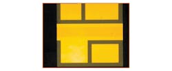
The layer thicknesses for the adhesion and barrier layers should be typically in the range of 80 to 200 nm. The gold termination layer is usually thicker, from 500 to 1,000 nm, for soldering purposes, and sometimes as thick as 2,000 to 3,000 nm for devices requiring high current levels. With the inherent insulating property of diamond, the generation of patterned metallization is possible, allowing a wider functionality of the heat spreader to also act as a submount for additional device mounting and/or wire-bond termination pads. Figure 3 shows an example of a CVD diamond heat spreader with patterned metallization.
3. This is an example of a heat-spreader design metallized on CVD diamond.
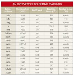
As with the metallization layers, soldering layers for attaching devices to the heat spreader should be kept at minimum thicknesses for optimum thermal dissipation. This is particularly true for the primary interface (TIM1) between device and heat spreader, again to minimize thermal resistance. For good results, predeposited solder materials, such as eutectic gold/tin (AuSn, at Tm = +278°C) or gold/germanium (AuGe, at Tm = +361°C), can be used. They are typically sputter-deposited or evaporated onto the heat spreaders at thicknesses of 2 to 4 µm. With a suitably designed die-attach process, the resulting solder layers should be void free and only a few microns in thickness.
Lastly, since diamond is capable of extreme heat transfer with an optimized primary interface, even the secondary thermal interface (TIM2) between the heat spreader and submount surface or package is important. The use of thermal pads or epoxy-type bonds, which have high thermal resistance, would impede the flow of heat. As a result, lower-melting-temperature solder materials like indium (In) or indium/tin (InSn) should be used. The soldering sequence is usually designed so that the most critical TIM1 interface is formed first, so as to mount a semiconductor chip on a heat spreader, which is then soldered into a package in a second step at a lower soldering temperature.
An alternative assembly approach is to use the same solder material for both sides of the heat spreader and attaching the device/heat-spreader package stack in one operation. In any case, when soldering, the mismatch in the coefficient of thermal expansion (CTE) between the CVD diamond and the semiconductor material must be considered. Gallium-arsenide (GaAs) semiconductor devices to an edge length of 2.5 mm can be attached with hard solder material to CVD diamond without CTE-mismatch problems. For larger devices, the use of soft solder material is recommended to avoid excessive stress that could jeopardize device performance or reliability. The table shows a wide range of solder materials commercially available for device soldering processes.
The thickness of CVD diamond can be important for thermal management. For a range of applications, a thickness of 250 to 400 µm is sufficient for thermal dissipation—particularly for small devices with high power densities. The isotropic characteristics of the diamond material help spread the heat efficiently, hence reducing the maximum operational temperature for a constant power output. However, for applications with larger heat spots on the order of 1 to 10 mm in diameter, the diamond thickness must be increased for better results. As an example, for disk lasers, which can generate several kilowatts of optical output power, the use of diamond with thickness of several millimeters has proven beneficial.
The electrical conductivity of the heat spreader can play a part in a device application. For some devices, the simplest design may involve running current through the device and the heat spread for a path to ground, as is often done with laser diodes. For other devices, the heat spreader may be used as an insulator. Since CVD diamond is an intrinsic insulator, its insulation properties can be maintained by keeping the side faces of the material free of metallization. This is required for RF/microwave amplifiers and transistors, especially at higher frequencies (greater than 2 GHz).
Modeling Thermal Flow
A head-spreader configuration is typically optimized for performance for a given power level by means of thermal simulation. Software simulation can help find the best solution based on output power, material thickness, metallization scheme, the geometry of the source of heat, and the package configuration.3 For best simulation results, it is important to model the complete system, including device details, interfaces, materials, and subsequent heat-sink approach, in performing a full junction-to-case thermal analysis.
To demonstrate the impact of a diamond heat spreader in a practical example, an RF amplifier design was analyzed. In this example, a VDMOS power amplifier package was initially made with a beryllium-oxide (BeO) heat spreader on a copper/molybdenum (CuMo) flange. The end user was interested in lowering the overall thermal resistance of the system design, as well as avoiding the use of BeO due to its toxicity. Modeling was performed with parameters for heat-spreader thermal conductivity and thickness using various soldering solutions.
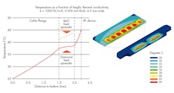
Figure 4 shows one of the key findings of this modeling and analysis. It demonstrates the junction-to-case temperature profile for one of the optimal designs. The CVD diamond heat spreader solution exhibited 30% lower thermal resistance at 0.300 mm thickness with thermal conductivity of 1,000 W/m-K (the original solution used a 1.00-mm-thick BeO heat spreader). Note the almost-horizontal, constant temperatures within the CVD diamond, which indicate that the heat spreader is not even employed to its full capability. But even so, the improved thermal resistance of the diamond heat spreader has led to this device functioning with better linearity and with improved reliability due to its reduced junction temperature.
4. Thermal modeling revealed the effectiveness of CVD diamond heat-spreader materials compared to other materials in an example application.
One important finding was the need to modify device architecture for improved thermal flow. The main temperature rise is within the device itself. A thinning of the device substrate, to bring it closer to the diamond heat spreader, would enhance the thermal design significantly. Also, mounting such devices with the active layers facing the diamond heat spreader would provide even further benefit, such as mounting laser diodes p-face down with the quantum well structures soldered directly against the heat spreader.
Another way to bring the device gate junction closer to the diamond is the use of a different substrate altogether. This has been demonstrated by using GaN-on-diamond wafers, which remove both the Si substrate and transition layers, replacing them instead with CVD diamond. The result brings the diamond material within 1 µm of the heat-generating gate junctions. Initial users of GaN-on-diamond wafers for RF HEMT devices have demonstrated as much as 3.5 times the power density compared to equivalent GaN-on-SiC devices.
Diamond materials can also be a useful allay in removing heat as part of package designs. CVD diamond can be embedded in copper/tungsten (CuW), copper/molybdenum (CuMo), or other packaging materials for enhanced thermal dissipation. This package design improvement cost-effectively decreases the thermal resistance of the thermal path between the device gate junction and the package case.
Significant improvements in the thermal design of electronic systems can be realized by using advanced materials such as CVD diamond. Integration of the material is relatively straightforward, since diamond heat spreader can serve as a direct replacement for aluminum nitride (AlN), BeO, or other ceramic materials. Attention to detail at the interfaces is important to keep overall thermal resistance low and optimize the effectiveness of the diamond for thermal dissipation. For example, once the thermal resistance of the TIM1 (primary thermal interface material) is minimized, attention must be turned to the secondary thermal interface (TIM2) as the limitation to the overall system performance.
Improved synthesis and processing techniques are making CVD diamond materials more available and affordable as head spreaders for electronic circuits. The trend in building denser electronic circuits with higher power levels per square inch is expected to continue, adding to the need for better thermal materials to prevent heat from degrading performance and reliability.
Thomas Obeloer, Business Development Manager
Daniel Twitchen, Head of CVD Business Development
Element Six Technologies, 3901 Burton Dr., Santa Clara, CA 95054
References
1. D.J. Twitchen, C.S.J. Pickles, S.E. Coe, et al., “Thermal Conductivity Measurements on CVD Diamond,” Diamond and Diamond Related Materials, Vol. 10, Nos. 3-7, March 2001, pp. 731-735.
2. C.D. Iacovangelo, “Thermal Stability of Metallized CVD Diamond,” Thin Solid Films, Vol. 286, Nos. 1-2, September 1996, pp. 264-269.
3. P.M. Fabis, D. Shum, and Henry Windischmann, “Thermal modeling of diamond-based electronics packaging,” IEEE Semiconductor Thermal Measurement and Management Symposium, Vol. 15, March 1999, pp. 98-104.

