Analyze RF JFETs for Large-Signal Behavior
This file type includes high-resolution graphics and schematics when applicable.
Linear amplification is a requirement for processing many waveforms, although achieving high amplifier efficiency with linear performance might present a challenge. For example, terminating a JFET in an optimum resistance (Ropt) at one-half the maximum current, or Vdc/(Imax/2), does not result in linear amplification with 50% efficiency.1 For that reason, it is necessary to reconsider the way that FETs are analyzed. Linear models cannot be used—one must first solve the equations that describe a JFET’s behavior to better understand and improve the performance.
In designing a linear, Class A amplifier, load-line analysis assumes that when the signal to a JFET’s gate is sinusoidal, the drain current and voltage will also be sinusoidal in nature. As a result, that approach cannot be used for a FET amplifier. In a FET, when the drain voltage is greater than or equal to a saturated drain voltage (Vdsat), where Vdsat is the voltage at which pinchoff occurs, then the drain current of an n-type JFET can be found by Eq. 1:
Ids = G0(Vg – Vp – (2/3)(Vbi – Vp){1 – [(Vbi – Vg)/(Vbi – Vp)]3/2}) (1)
where G0 is the conductance of the FET channel when there is no depletion layer; Vg is the gate voltage; Vp is the pinchoff voltage; and Vbi is the “built-in” p-n junction potential.2
It can be seen from Eq. 1 that when Vg is a sinusoid, drain current Ids contains harmonics; therefore, load-line analysis cannot be used. At saturation, Ids is solely a function of the gate voltage. Equation 2 provides a good approximation for the drain current:
Ids = Idss(1 – Vg/Vp)2 (2)
where Idss is the saturated drain current when the gate voltage is zero, Vg = 0.
When the gate voltage is set for a maximum value of zero and minimum value of Vp, the gate voltage can be found with Eq. 3:
Vg = (Vp/2)[1 – Kcos(ωt)] (3)
where K = 1. Substituting Eq. 3 into Eq. 2, with K = 1, yields Eq. 4:
Ids = Idss[3/8 + (1/2)cos(ωt) + (1/8)cos(2ωt)] (4)
The dc power can be determined by Eq. 5:
P0 = (3/8)IdssV0 (5)
while the output power at the fundamental frequency (P1) can be found using Eq. 6:
P1 = I12Ropt/2 = (Idss/2)2Ropt/2 = Idss V0/4 (6)
where Ropt = V0/(Idss/2) is the load resistance thought to be the optimum value1 as determined by load-line analysis when setting the “knee voltage” equal to zero. Parameter I1, which is the magnitude of the current at the fundamental frequency, is equal to Idss/2 as indicated by Eq. 4. Equations 5 and 6 yield an efficiency of 66.7% when calculating P1/P0. The efficiency is greater than 50% due to the second-harmonic current consumption, thus decreasing the magnitude of the dc current. Since the amplifier has second-harmonic components of both current and voltage, it is not linear.
Current Ids is a function of gate voltage Vg and not of the load impedance. If the load impedance presents a short-circuit condition at the second-harmonic frequency, only the fundamental frequency will appear at the output of the amplifier. In order for the drain voltage to always be greater than or equal to the saturated drain voltage Vdsat, the optimum load resistance RL will be represented by Eq. 7:
RL = 2(V0 – |Vp |)/Idss (7)
The fundamental-frequency output power (P1) is given by Eq. 8:
P1 = I12RL/2 = Idss(V0 – |Vp |)/4 (8)
and the efficiency by Eq. 9:
Eff = (2/3)(V0 – |Vp |)/V0 (9)
Substituting Eq. 2 into Eq. 3, the output current at the fundamental frequency (I1) is equal to 0.5(Idss)Kcos(ωt). Thus, the output voltage (I1RL) and the input voltage at the fundamental frequency, given by Eq. 3, are linearly related, indicating that the amplifier is truly linear.
Large-signal nonlinear analysis based on device physics must be performed to arrive at the correct solution for a FET model. Unfortunately, many incorrect waveforms result from using linear models. The FET channel must be treated as a resistance that is a function of the gate voltage, and the drain voltage and current follow Ohm’s Law, or I(t) = V(t)/R(t). If at any time (t0) the drain voltage is equal to zero, then the drain current must also be equal to zero at that time. Any set of waveforms in which drain current flows when the drain voltage is zero is not possible with a FET, including Class E and F waveforms.
The “Grayzel JFET”
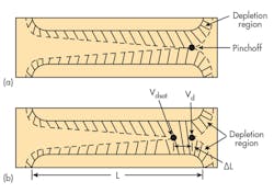
When the drain voltage of a JFET is exactly equal to Vdsat, the conditions are those of Fig. 2a,2 where pinchoff occurs exactly at the drain of the transistor. If the drain voltage is increased by ΔV, the point at which pinchoff occurs moves toward the source a distance of ΔL (Fig. 2b).
Over the length ΔL, at the drain, the voltage is completely depleted. Only minority carriers remain and the resistance is quite large. Voltage ΔV drops across this depleted region and, due to the high resistivity in the depleted region, ΔL is very small. For ΔL << L, which represents the usual case, the depletion from source to pinchoff point will be essentially identical in shape and have effectively the same resistance from the source to the point where pinchoff occurs.2 There is hardly any change to drain current, which is equal to Vdsat divided by this resistance. This explains why the value of the drain current is nearly constant for drain voltages greater than Vdsat.
The instantaneous power P(t) dissipated in the depleted region is equal to Id(t)ΔV(t). Integrating this product over a cycle setting of ΔV(t) = 0 for ΔV(t) < 0 yields the total dissipated power in the totally depleted region. In addition, ohmic losses develop in the portion of the channel that is not totally depleted.
Since voltage ΔV(t) drops across the depleted region ΔL, it does not contribute to the output power and simply degrades the efficiency. It is therefore clear that, for high efficiency, the depletion region must be minimized. Ideally, when converting dc power to RF power, the channel should have no depletion at all for one-half the cycle and should be completely cut off for the other one-half cycle. With the optimum load, this should yield the maximum dc-to-RF efficiency. To accomplish this, a new (patented) FET model is presented that will be referred to as the “Grayzel JFET.”
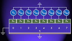
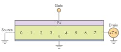
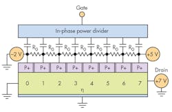
Figure 3 shows a simplified schematic of a JFET with a drain voltage of 7 V dc. Along the channel, the potential has values of 0, 1, 2, 3, 4, 5, 6, and 7 V. The junction is progressively back-biased, causing greater depletion at the drain than at the source. Fig. 4 shows a simplified schematic diagram of the “Grayzel JFET.” The P+ region is divided into N sections that are insulated from one another, forming N p-n junctions. (In Fig. 4, N is equal to 8 as an illustrative example.)
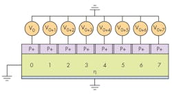
Each p-n junction is biased to ground separately as shown in Fig. 4—the first at V0 and the eighth at V0 + 7. With a drain voltage of 7 V, all of the p-n junctions will have the same dc voltage V0 across their junctions and hence, to a good approximation, all of the junctions will act in unison.
Consider as an example of a Grayzel JFET a device where all p-n junctions are completely depleted when back-biased with a voltage of –4 V dc. The gate voltage is then equal to –4 V dc, and the drain current is approximately zero. A square wave varying from –2 to +2 V is applied to each of the p-n junctions through an eight-way, in-phase power divider (Fig. 5). The p-n junctions are biased such that each p-n junction has a bias voltage of –2 V dc when the drain voltage is equal to 7 V dc. The channel will be without depletion for about one-half of the cycle and cutoff for approximately the other one-half. For very large N, the conductance of the channel approaches an ideal square wave varying between 0 and G0, where G0 is the value of the conductance of the channel when there is no depletion region.
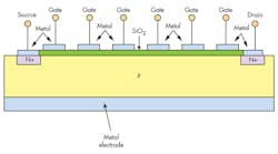
This p-n biasing arrangement represents just one example, though. The p-n junctions can be biased individually, as shown in Fig. 4, or by other means. The act of dividing the gate into multiple sections is applicable to all types of FETs. Fig. 6 shows an example of the Grayzel MOSFET with the gate divided into N sections, with N = 6.
Special Case
One might also want to consider a special case for the Grayzel JFET: In this instance, odd-order harmonics are short-circuited and the even-order harmonics are open-circuited. In addition, for one-half of the cycle, the JFET is cut off; for the other half of the cycle, the depletion region in the channel is of minimal width. The conductance is thus a square wave varying between 0 and G0, where G0 is the conductance when the depletion region in the channel is of minimal width. If θ = 2πft = ωt, where f represents the fundamental frequency of the square wave, the Fourier series of the square wave can be given by Eq. 10a:
G(t) = 0.5G0 + g(t) (10a)
where:
g(t) = (2G0/π)( cosθ – cos(3θ)/3 + cos(5θ)/5 – cos(7θ)/7 +….
= (2G0/π)Σ∞k = 1(–1)k–1 cos[(2k – 1)θ]/(2k – 1) (10b)
The FET is terminated in an admittance Y(ω), which at the fundamental frequency has a value GL. The value of Y(ω) is zero at the even harmonics and infinite at the odd harmonics of the fundamental frequency. The drain voltage, therefore, has only even harmonics and the drain current has only odd harmonics. The drain voltage, Vd(t), is chosen to take the form of Eq. 11a:
Vd(t) = V0 + v(t) (11a)
where:
v(t) = V1 cos(θ) + Σ∞k = 1 (V2k)cos(2kθ) (11b)
This form was chosen for the following reason: According to Eq. 10, the value of the conductance of the channel is equal to G0 when –90° < θ < +90° and the channel is cut off for the remainder of the cycle. As a result, current will only flow when –90° < θ < +90°. Since the current is equal to Vd(t)G(t), Vd(t) will have its maximum value centered at θ = 0° and will thus be equal to the sum of cosines.
The bias voltage V0 in Eq. 11a is the same for all of the p-n junctions, with the Grayzel JFET progressive-biased as described earlier. There will, however, be a variation of the depletion region along the channel due to v(t) in Eq. 11a. This variation will be small and is neglected in this analysis.
The amplifier shown in Fig. 7a, where the FET is a Grayzel JFET, will be analyzed with the aid of the circuit in Fig. 7b. Voltage v(t), given by Eq. 11a, appears across the RF choke in series with the dc battery, across the load GL in series with blocking capacitor C, and across the nonlinear susceptance G(t) given by Eq. 10a. The choke, which is in series with the dc battery, has voltage v(t) across it, but negligible RF current flowing through it. Drain current Id(t) = I0 + i(t) is equal to the product G(t)[Vd(t)]. Current i(t) flows in a loop through the termination Y(ω) (Fig. 7). In turn, dc voltage V0 is dropped across the blocking capacitor C.
The drain current is given by Eq. 12a:
Id(t) = [V0 + v(t)][0.5G0 + g(t)]
= 0.5V0(G0) + V0[g(t)] + 0.5G0[v(t)]+v(t)g(t)
= 0.5V0(G0) + v(t)g(t)
+ V0[(2G0/π)( cosθ – cos(3θ)/3 + cos(5θ)/5 – cos(7θ)/7+….)
+ 0.5G0(V0)(V1 cosθ + V2cos(2θ)+ V4cos(4θ) + V6cos(6θ)+…] (12a)
where:
v(t)g(t) = (V1 cosθ)(2G0/π)(cosθ – cos(3θ)/3 + cos(5θ)/5 – cos(7θ)/7 + ...)
+ (V2 cos2θ)(2G0/π)(cosθ – cos(3θ)/3+ cos(5θ)/5 – cos(7θ)/7 + …)
+ (V4 cos4θ)(2G0/π)(cosθ – cos(3θ)/3+ cos(5θ)/5 – cos(7θ)/7 + …)
+ (V6 cos6θ)(2G0/π)(cosθ – cos(3θ)/3+ cos(5θ)/5 – cos(7θ)/7 + … (12b)
The drain current can therefore be written as the sum of the dc term, the odd harmonics, and the even harmonics:
Id(t) = I0 + Σ∞k = 1 (I2k – 1)cos(2k – 1)θ + Σ∞k = 1(I2k)cos(2k)θ (13)
Using the identity cos(x)cos(y) = 0.5[cos(x + y) + cos(x – y)], the even harmonics can be found from Eq. 12 by means of Eq. 14:
I2k = G0{0.5V2k – (2V1/π)(–1)k /[(2k – 1)(2k + 1)]} (14)
Since the currents at the even harmonics are zero, it is possible to solve for voltage V2k by setting current I2k equal to zero in Eq. 14, thus yielding Eq. 15:
V2k = (4/π)(V1)(–1)k/[(2k – 1)(2k + 1)] (15)
Collecting the terms in cosθ in Eq. 12, the value of the current at the fundamental frequency I1 can be found by Eq. 16:
I1 = (G0){2(V0)/π + 0.5(V1) – (2/π) Σ∞k = 1(–1)kV2k /[(2k–1)(2k+1)]} (16)
Substituting Eq. 15 into Eq. 16 yields Eq. 17a:
I1 = (G0)(2(V0)/π+V1 (0.5 – (8/π2)Σ∞k = 1{1/[(2k–1)(2k+1)]}2) (17a)
The term (0.5 – (8/π2) Σ∞k = 1{1/[(2k–1)(2k+1)]}2) was found to converge in the limit to (π/2)2 as k approaches infinity. (This limit was first estimated and then verified by computer program.) Substituting for (0.5 – (8/π2)Σ∞k = 1{1/[(2k-1)(2k+1)]}2), the limit (π/2)2
in Eq. 17a yields Eq. 17b:
I1 = G0[2(V0)/π + (2/π)2V1] (17b)
At the fundamental frequency Y(ω) = GL, and as can be seen from Fig. 7, I1 = –(GL)(V1).
By equating I1 as given by Eq. 17b to –(GL)(V1):
2(G0)(V0)/π + (G0)(V1)(2/π)2 = –(GL)(V1) = –(X)(G0)(V1) (18)
where X= GL/G0. Solving Eq. 18 yields Eq. 19:
V1 = –(2/π)(V0)/[X+ (2/π)2] (19)
The dc current I0 is found from Eq. 12 to have two terms. The first term is 0.5(G0)(V0). The second dc term results from the product [(2G0/π)cosθ](V1cosθ) and is equal to (G0)(V1)/π. Thus,
I0 = 0.5(G0)(V0) + (G0)(V1)/π = 0.5(G0)(V0)(1 + (2/π)/V1/V0) (20a)
Substituting Eq. 19 into Eq. 20a yields:
I0 = 0.5(G0)(V0)(X)/[X+(2/π)2 ] (20b)
The efficiency of the Grayzel FET model for this special case can be found in the following way. The dc power is equal to (I0)(V0). Multiplying Eq. 20b by voltage V0 yields Eq. 21:
P0 = (I0)(V0) = 0.5(G0)(V0)2(X)/[X+(2/π)2] (21)
The output power at the fundamental frequency P1 is found by Eq. 22:
P1 = 0.5(GL)(V1)2 = [2(V0)2(GL) /π2]/[X+(2/π)2]2 (22)
The efficiency (EFF) is then:
EFF = P1/P0 = (2/π)2/[X+(2/π)2 ] (23a)
and the efficiency (to three-places accuracy) is:
EFF = P1/P0 = 0.405/(X + 0.405) (23b)
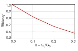
Figure 8 shows a plot of efficiency as a function of X as given by Eq. 23. This special case where the amplifier is terminated in an open circuit for even harmonics and a short circuit for odd harmonics gives good results. However, it isn’t necessarily an optimum termination. An analysis similar to what was performed here, but where the amplifier is terminated in an open circuit for odd harmonics and a short circuit for even harmonics, gave a poorer result. Optimization is required to determine an optimum termination.
Acknowledgments
The author wishes to acknowledge the support given by Dr. Ashok Gorwara, CEO of Planar Monolithics Industries Inc. (PMI), and support provided by the staff of PMI.
Dr. Alfred Grayzel is a consultant for Planar Monolithic Industries Inc., 7311 Grove Rd., Ste. F, Frederick, MD 21704; (301) 662-5019.
References
1. Steven C. Cripps, RF Power Amplifiers For Wireless Communications, 2nd ed., Artech House, Norwood, MA, 2006, pp. 22-24.
2. R.F. Pierret, Field Effect Devices. Modular Series on Solid State Devices, Addison-Wesley Publishing Company, Boston, MA, 1983, pp. 5-15.
