I/Q Demodulator Processes 1-GHz Bandwidths to 6 GHz
This file type includes high-resolution graphics and schematics when applicable.
Demodulation of wideband communications systems becomes more challenging with the arrival of every new wireless standard and every next generation of cellular communications system. Fortunately, the model LTC5586 in-phase/quadrature (I/Q) demodulator from Linear Technology helps mitigate the situation by providing the demodulation bandwidth necessary to satisfy emerging wideband requirements.
With a frequency range of 500 MHz to 6 GHz (and 300 MHz to 6 GHz by adding an external matching capacitor), this zero-intermediate-frequency (zero-IF) demodulator features an IF bandwidth of dc to 1 GHz with amplitude flatness of ±1 dB. Its wide bandwidth and high-performance analog signal processing ease the requirements for analog-to-digital converters (ADCs) at the demodulator’s I and Q output ports, supporting practices such as digital predistortion (DPD) to improve transmitter linearity. The demodulator essentially has what it takes to design receivers for next-generation wireless communications systems, including Fifth-Generation (5G) cellular infrastructure systems.
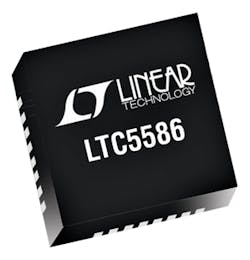
The LTC5586 (Fig. 1) is a densely packed integrated circuit (IC) supplied in a surface-mount-technology (SMT) housing. Since it uses quadrature demodulation, wideband modulation can be achieved within its 1-GHz IF bandwidth without requiring extensive digital signal processing (DSP) of demodulated I and Q outputs to maintain signal linearity. As a result, the demodulator can be paired with lower-cost DSPs and field-programmable gate arrays while still maintaining excellent performance with wideband carriers through 6 GHz.
Subsystem on a Chip
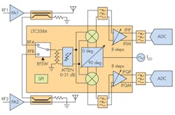
The LTC5586 incorporates I and Q mixers; I and Q IF amplifiers with eight gain settings and maximum gain of 7.7 dB at 1.9 GHz; an RF attenuator with as much as 31-dB attenuation, adjustable in 1-dB steps; and a two-channel single-pole, double-throw switch with 40-dB isolation and 100-ns switching speed for selecting input signals (Fig. 2). In addition, the demodulator provides a serial peripheral interface (SPI) to control the local-oscillator (LO) input to any frequency band from 300 MHz to 6 GHz without external matching components. The demodulator’s I and Q outputs can drive filters and external ADCs when terminated with external 100-⦠differential impedance.
The wideband demodulator achieves typical –70-dBc image rejection at 3.5 GHz. The extremely linear device features output third-order-intercept (OIP3) performance of typically +35 dBm and output second-order-intercept (OIP2) performance of typically +70 dBm, both measured at 3.5 GHz.
The LTC5586, housed in a 5- × 5-mm plastic 32-lead QFN package, is designed to maintain consistent, reliable performance over operating temperatures from –40 to +105°C. To ensure optimum results, the demodulator includes on-chip calibration of the amplitude and phase responses of its I and Q channels. Calibration and other functions are controlled via the SPI connection.
This novel use of on-chip fine-tuning can make adjustments for deviations in amplitude and phase between the I and Q channels, helping to improve the demodulator’s image-rejection performance. Performing these adjustments in the analog realm greatly reduces requirements for such corrections in the digital realm, along with reduced-speed requirements for DSPs and FPGAs at the demodulator’s outputs. The LTC5586 has the potential to be a key building block in simpler, less-expensive, wideband 5G receiver solutions.

About the Author
Jack Browne
Technical Contributor
Jack Browne, Technical Contributor, has worked in technical publishing for over 30 years. He managed the content and production of three technical journals while at the American Institute of Physics, including Medical Physics and the Journal of Vacuum Science & Technology. He has been a Publisher and Editor for Penton Media, started the firm’s Wireless Symposium & Exhibition trade show in 1993, and currently serves as Technical Contributor for that company's Microwaves & RF magazine. Browne, who holds a BS in Mathematics from City College of New York and BA degrees in English and Philosophy from Fordham University, is a member of the IEEE.
