This file type includes high-resolution graphics and schematics when applicable.
Millimeter-wave frequencies offer wide available bandwidth for short-range communications at high data rates. Today, due to the relentlessly increasing consumption of bandwidth for broadcast, wireless devices, and other applications at lower frequencies, millimeter-wave bands have been pushed into the spotlight. For instance, they are gaining significant footholds as possible solutions for backhaul data links from base stations in various fifth-generation (5G) cellular networks (still in the planning stages).
Of course, millimeter-wave radar devices are being employed in some automotive safety (collision-avoidance) systems. And many proposals for 5G point to a mass consumer-level use of frequencies once regarded as the sole realm of scientific or military applications.
The main—and what’s become long-term—obstacle in bringing such high frequencies (above 30 GHz) to the masses is the implementation of millimeter-wave circuits and devices at reasonable (affordable) costs. To overcome that hurdle, and open the door to possible widespread use of millimeter-wave technology, fabless semiconductor company Anokiwave adopted a flexible design approach: Devices are fabricated at outside foundries using the semiconductor process deemed the best fit for a particular function and application, such as gallium arsenide (GaAs) for small-signal, low-noise, and medium-power amplification.
Silicon-based device processes such as silicon germanium (SiGe) and silicon CMOS are an important part of Anokiwave’s device process portfolio. They enable the firm to produce practical, high-performance integrated circuits (ICs) for a wide range of markets, from communications to radar systems.
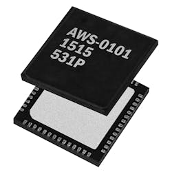
The company’s name derives from “Anoki,” the Hindi word for “extraordinary” and “unique.” The ISO 9001:2008 certified company has locations in San Diego, Calif., as well as Phoenix, Ariz. and Boston, Mass. Along with its millimeter-wave devices, the company has introduced a number of X-band monolithic microwave integrated circuits (MMICs) for active electronically steered array (AESA) applications, including the model AWS-0101, a quad-core integrated circuit (IC) with transmit and receive functions from 8 to 11 GHz (Fig. 1).
Targeting X- and K-Bands
The AWS-0101 supports four radiating elements, each capable of dual polarization, for electronic beam steering in phased-array radar and communications systems. Based on a SiGe semiconductor process, it provides 21-dB gain for both transmit and receive, with +15-dBm transmit output power at 1-dB compression and 3.4-dB receive noise figure.
For programming fast beam-steering operation, it includes 6-b amplitude control with least significant bit (LSB) of 0.5 dB and 6-b phase control with LSB of 5.625 deg. The power-efficient device consumes only 1.8 W in transmit mode and 1.8 W in receive mode when operating from a low-voltage, +1.8-V dc supply.
The X-band transmit/receive IC is ideal for commercial and weather radar systems and 5G communications systems using AESAs. It comes in a 56-lead, 7- × 7-mm PQFN package with an operating temperature range of –40 to +85°C. The lead-free device is fully RoHS-compliant.
Moving higher in frequency, model AWS-0102 is another quad-core IC, designed for K-band satellite-communications (satcom) receiver systems. It also supports four radiating antenna elements, each with dual polarization, from 17.7 to 20.2 GHz. The receiver IC is quite flexible in these applications, and can be used for linear polarization as well as left-handed (LH) and right-handed (RH) circular polarization (CP).
The AWS-0102 offers 22-dB coherent channel gain with 3.4-dB noise figure. It features programmable 5-b control of phase and gain, with 11.25-deg. phase resolution and 5-deg. root-mean-square (RMS) phase error, and 15.5-dB dynamic range for gain with 0.5-dB resolution and 0.25-dB RMS amplitude error.
Also housed in a 56-lead, 7- × 7-mm PQFN package for ease of installation in planar phase-array antennas, the SiGe IC includes temperature-sensing circuitry for stable performance over a temperature range of –40 to +85°C. The device includes electrostatic-discharge (ESD) protection on all package pins. It consumes just 0.3-W power from a +1.8-V dc supply.
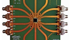
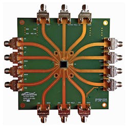
To help circuit designers get started with its quad-core ICs, the firm offers Developer Kits for all of its ICs, which include numerous interfaces to facilitate testing (Fig. 2). Each kit contains a test circuit board that helps emulate the operation of the device in actual applications and provides high channel-to-channel isolation to view channel characteristics separately. Calibration data is also included, to subtract circuit-board and connector losses from the device itself when testing.
Each kit and board offers Serial Peripheral Interface (SPI) control via a high-speed cable, interposer board, and Universal Serial Bus (USB) interface module. In addition, drive software is included to control device functions with a personal computer (PC) during evaluation and testing. A separate cable assembly supplies dc power to the test board. Each Developer Kit features its own set of measured data to serve as reference points for users to compare their own measured results.
Ka-Band Transceiver
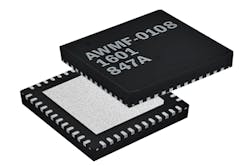
The quad-core design approach was also applied to higher frequencies, specifically in the model AWMF-0108 transceiver (Fig. 3) nominally for 5G antenna arrays. The Ka-band device operates from 27.5 to 30.0 GHz.
As with the AWS-0101 transceiver, the AWMF-0108 supports radiating elements in antenna arrays with healthy transmit and receive gain. The half-duplex transceiver is capable of fast beamsteering and telemetry reporting, with programmable amplitude and phase control. In a 5G system, for example, it could be used in a 4 × 4 configuration of AWMF-0108 devices as part of an AESA solution for a compact 64-element planar antenna array, with the flexibility of electronic beamsteering that eliminates the need for mechanical motion of an antenna.
The model AWMF-0108 transceiver achieves 26-dB transmit gain with +9-dBm transmit output power at 1-dB compression. It also features 31-dB coherent receive gain with 4-dB noise figure and –23-dBm receive input third-order-intercept point (IIP3). Beamsteering is performed with 5-b phase control with LSB of 11.25 deg., and 5-b gain control with 1-dB amplitude resolution.
Designed to operate from a +1.8-V dc supply, the device consumes 0.65 W power in quiescent transmit mode, 0.85 W at transmit 1-dB compressed output power, and 0.50 W in receive mode. The Ka-band transceiver is supplied in a 48-lead, 6- × 6-mm PQFN package with ESD protection on all pins.
Reaching E-Band
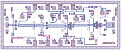
These are just a sampling of the firm’s silicon-based devices at “lower” frequencies. Anokiwave has announced many more upcoming introductions, including models AWP-7176 and AWP-8186—GaAs power amplifiers (PAs) developed for E-band point-to-point communications (Fig. 4). Model AWP-7176 operates from 71 to 76 GHz, while model AWP-8186 boosts signals from 81 to 86 GHz.
Both PAs feature a five-stage circuit architecture, each capable of +25-dBm typical saturated output power across their full frequency ranges. The tiny devices (2.90 × 2.29 mm), which include on-chip, diode-based forward power detectors, offer flexible dynamic ranges of +18 to +30 dBm while drawing only 900 mA at +3.5 V dc.
With a little more power at somewhat lower frequencies, model AWP-1102 is a PA for satcom, AESA, and point-to-point-communications applications at Ka-band frequencies from 28 to 30 GHz. It provides 25-dB linear gain across the 2-GHz bandwidth with +34.6-dBm (3-W) saturated output power. The four-stage PA is fabricated in a 0.15-µm pseudomorphic GaAs high-electron-mobility-transistor (pHEMT) semiconductor process. It draws 2.9 A current from a +6-V dc supply and comes in a 28-lead, 5- × 5-mm QFN package.
For receiver applications at E-band, the firm also offers the model AWL-7186 low-noise amplifier (LNA), with better than 3.5-dB noise figure from 71 to 86 GHz. The four-stage amplifier provides typical gain of 17 dB across the 15-GHz bandwidth, with an adjustable gain range of 15 dB. Gain is controlled by applying –2.6 to –1.8 V dc in 0.2-V steps. Representing one part of the company’s blend of devices based on different semiconductor processes, the LNA also leverages a 0.1-µm pHEMT process for excellent high-frequency performance. It generates +8 dBm output power at 1-dB compression and has an operating temperature range of –20 to +85°C. Supplied in die form that measures 2.90 × 1.12 mm, the LNA maintains typical current draw of 80 mA at +3.5 V dc.
As with 5G, some of these higher-frequency devices are still in the testing and evaluation stages, with near-term product availability. In general, the devices are RoHS-compliant and durable, with ESD protection and power-monitoring functions where appropriate. They provide a glimpse into the design philosophy of a company poised to embrace the challenges of affordable communications and radar functions at millimeter-wave frequencies. Moreover, it’s a firm positioned to supply the devices needed for 5G systems should they incorporate data links at millimeter-wave frequencies.
Anokiwave Inc., 12555 High Bluff Dr., San Diego, CA 92130; (781) 820-1049, e-mail: [email protected].
Looking for parts? Go to SourceESB.
About the Author
Jack Browne
Technical Contributor
Jack Browne, Technical Contributor, has worked in technical publishing for over 30 years. He managed the content and production of three technical journals while at the American Institute of Physics, including Medical Physics and the Journal of Vacuum Science & Technology. He has been a Publisher and Editor for Penton Media, started the firm’s Wireless Symposium & Exhibition trade show in 1993, and currently serves as Technical Contributor for that company's Microwaves & RF magazine. Browne, who holds a BS in Mathematics from City College of New York and BA degrees in English and Philosophy from Fordham University, is a member of the IEEE.
