Bias Module Keeps GaN Devices Protected

This file type includes high resolution graphics and schematics when applicable.
Gallium-nitride (GaN) power transistors and integrated circuits (ICs) have caught on quickly for large-signal applications in commercial and military systems. The technology offers impressive power levels through RF and microwave frequencies. But developing power supplies for this advanced semiconductor technology is not always routine, until now.
MACOM, well-known for its GaN-based devices, has introduced a GaN bias controller and sequencer for fixed and pulsed negative gate biasing of GaN semiconductor devices. The power-supply module makes it easier to turn on (or off) a GaN semiconductor device by providing the proper gate and drain bias voltages. The module actually contains two voltage supplies, with the negative source capable of providing -8 to -3 VDC and the positive supply with an adjustable range from +12 to +55 VDC.
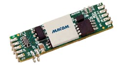
The model MABC-001000-DP000L GaN bias controller and sequencer module (see figure) is much more than a dual-voltage supply, however. It is designed to protect GaN devices by ensuring that voltages are supplied in the proper sequence: the module will not allow a pulsed drain-source voltage to be applied to a device under test (DUT) unless the negative gate bias has already been applied. The bias controller module can be used with all of the firm’s high-power transistors, including its broad line of GaN devices. It is well suited for powering depletion-mode GaN and gallium-arsenide (GaAs) power transistors and IC amplifiers.
The module is constructed of two functional elements, essentially the drain and gate supplies for a DUT. These functional elements can be arranged vertically on a customer’s test board to save space and cost. The MABC-001000-DP000L module can also be installed onto an MABC-001000-PB1PPR evaluation board as required for evaluation, test, and characterization purposes.
The first functional element is patterned and fabricated onto a customer’s test board or onto the standard MACOM evaluation board. The second functional element uses the land pattern of the first functional element and interconnects vertically through the first functional element. The first functional element provides drain voltage switching while the second functional element simplifies gate switching to a GaN or other active DUT.
This bias module provides protection through proper voltage sequencing but also provides high-speed bias sequencing, with a total switch transition time of better than 500 ns. It is capable of open drain output current of as much as 200 mA and gate bias output current of as much as 50 mA. An internal thermistor or external temperature sensor voltage can be used to monitor the gate bias as a function of changing temperature under operation, and the model MABC-001000-000DPM bias module is both RoHS compliant and +260°C reflow solder compatible is designed for use in environments with heavy radio-frequency interference (RFI) and electromagnetic interference (EMI) as required, with typical EMI/RFI rejection of 30 dB at all ports.
According to Gary Lopes, MACOM’s senior product director, “The MABC-001000-DP000L is ideal for a DUT such as depletion-mode GaN or GaAs power amplifiers, or HEMT devices.” He added that “in addition to these key applications, this device can be used for high power transistors including LDMOS, silicon bipolar, and more.” In a standard configuration, the MABC-001000-DP000L bias module measures 6.60 × 22.48 mm and can handle operating temperatures from -40 to +85°C.
MACOM Technology Solutions, Inc., 100 Chelmsford St., Lowell, MA 01851; (978) 656-2500.
This file type includes high resolution graphics and schematics when applicable.
About the Author
Jack Browne
Technical Contributor
Jack Browne, Technical Contributor, has worked in technical publishing for over 30 years. He managed the content and production of three technical journals while at the American Institute of Physics, including Medical Physics and the Journal of Vacuum Science & Technology. He has been a Publisher and Editor for Penton Media, started the firm’s Wireless Symposium & Exhibition trade show in 1993, and currently serves as Technical Contributor for that company's Microwaves & RF magazine. Browne, who holds a BS in Mathematics from City College of New York and BA degrees in English and Philosophy from Fordham University, is a member of the IEEE.
