Designing AlGaN/GaN HEMTs for W-Band
This file type includes high resolution graphics and schematics when applicable.
Semiconductor devices such as AlGaN/GaN high-electron-mobility transistors (HEMTs) have attracted a great deal of attention for applications reaching through W-band frequencies. Such devices feature a high two-dimensional electron gas (2DEG) structure, high saturation drift velocity, high breakdown voltage, and good high-temperature resistance for use in high-frequency amplifier circuits. Millimeter-wave HEMTs have become a focal point for international research in recent years.1
Based on this background, a 2 × 50 μm AlGaN/GaN HEMT with 0.1-μm gate length and 2 μm between the source and drain is 2 μm was designed and simulated with the aid of the Technology Computer Aided Design (TCAD) computer-aided-engineering (CAE) software from Silvaco. The device was taped out using actual semiconductor processing technology, and the DC and signal characteristics were measured. A novel symbolically defined device (SDD) large-signal model was created which obtains excellent DC and S-parameter results. With this model, device large-signal characteristics can be known through source and load-pull simulations. The positive results for the model indicate that it is an effective tool for designing power amplifiers at W-band frequencies.
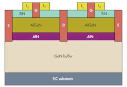
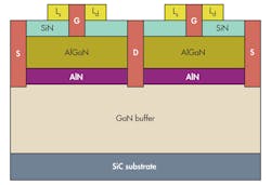
Figure 1 shows the cross-sectional structure of a double-finger AlGaN/GaN HEMT. The gate-length is 0.1 μm and the gate cap is 0.35 μm long. The silicon-nitride (SiN) passivation layer helps reduce surface defects and isolation boost electrode isolation. A single-finger gate width of 50 μm was used based on the principle that the phase difference be no more than π/16 at W-band frequencies. The distance between the source and drain is 2 μm and the lateral structure of the HEMT is symmetric.2 This contributes to lower channel series resistance and improved high-frequency characteristics.
The device heterostructure consists of a 1.5-μm-thick GaN buffer layer and a 23-nm-thick AlGaN barrier layer with 24% Al content. To enhance 2DEG channel characteristics, the AlN layer is inserted between the barrier layer and the 1-nm-thick buffer layer. All the vertical layers are unintentionally doped. The 2DEG mobility and sheet carrier concentration are 2000 cm2/V·s and 1.1 × 1013 cm-2, respectively. A silicon-carbide (SiC) substrate was chosen for its excellent thermal conductivity.
The 2DEG of AlGaN/GaN HEMTs is determined by polarization, which is described by Eq. 1:
where Psp represents spontaneous polarization for the GaN materials and Ppi is the piezoelectric polarization between AlGaN and GaN materials which is given by Eq. 2:
where α, C, and E represent lattice constants, elastic constants, and piezoelectric constants, respectively; their values can be obtained according to the material statement so that polarization can be calculated.3
The channel, regarded as a thin layer, is formed in the buffer layer approaching to surface of the barrier layer because of polarization effect. Empirical fitting function can be used to describe mobility models of the GaN channel.4
This file type includes high resolution graphics and schematics when applicable.
Field Analysis
This file type includes high resolution graphics and schematics when applicable.
For low-field analysis, the Farahmand Modified Caughey Thomas model depicted in Eq. 3 has been used:
where TL and N represent the junction temperature and doping concentration, respectively; and parameters A through F, M1, and M2 are fitting coefficients for the low-field model.
For high-field analysis, the model based on the Monte Carlo method and shown in Eq. 4 has been used:
where E represents electric field. Parameters VSATN, ECN, N1N, N2N, and ANN are fitting coefficients for the high-field model.
The current density of electrons and holes are defined to express change of lattice temperature (Eq. 5):
where q is quantity of electric charge. Parameters μn, n, φn, and Pn represent electron mobility, concentration, potential, and absolute thermoelectric power, while μp, p, φp, and Pp are the mobility, concentration, potential, and absolute thermoelectric powers for the semiconductor holes.
The total heat is a result of the sum of the Joule heating term, the recombination and generation heating and cooling term, and the Peltier and Joule-Thomson effects. The expression is described as follows5:
where R represents the heating recombination rate and G is the heating generation rate.
The TCAD software was used to simulate the HEMT; all of these physical models will be included in the design procedure. The work function of the gate metal was set 4.8 eV and the SBH can be ensured at 1.5 eV. The background doping concentrations of all the layers were set 1015 cm-3. The GaN buffer layer has exhibited high resistance characteristics and the mobility was set at 300 cm2/V·s.
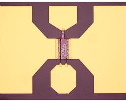
All epitaxial layers were grown on an SiC substrate by means of rapid thermal metal-organic chemical vapor deposition (MOCVD). Ti/Al/Ni/Au is evaporated to form the source and drain electrodes as a result of a rapid thermal anneal at +900°C for 35 s. A transmission-line matrix measurement method determined the ohmic contact resistant at 0.3 Ω-mm. The gate was formed by electronic-beam lithography and Ni/Au was chosen as the gate metal. Figure 2 shows a photo of the device fabricated after fabrication and fabrication process optimization.
This file type includes high resolution graphics and schematics when applicable.
Measured and Simulated Curves
This file type includes high resolution graphics and schematics when applicable.
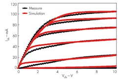
Figure 3 displays measured and simulated curves for Ids - Vds for the HEMT structure and device models. The gate voltage was simulated from -5 to 0 VDC and drain voltage from 0 to +10 VDC. The device channel enters the on-state at a gate voltage of -5 VDC, essentially the threshold voltage. The saturation drain current can reach 1.05 A/mm and the knee voltage is 5 V at a 0-VDC gate voltage. This indicates strong depletion-type characteristics for the HEMT device. Measurements indicate a current collapse effect for the HEMT, and further researching will be needed to solve this problem.
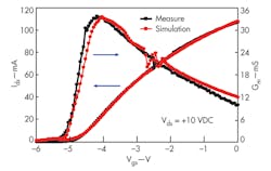
In the meantime, the Ids - Vgs and Gm - Vgs curves were measured and simulated, and are shown in Fig. 4. When the drain voltage is +10 VDC, the maximum transconductance may reach 338 mS/mm, and this peak value appears at a gate voltage of -4.2 VDC. The measured curves are close to the simulation curves, indicating the validity of the device simulation, and that the TCAD simulation technology is valuable for the design of AlGaN/GaN HEMTs.
The current gain cutoff frequency (fT) and maximum frequency of oscillation (fmax) are determined by the current gain (H21) and maximum available power gain (MAG), respectively, both calculated by the S-parameters according to Eqs. 7-9:
where K represents the stable factor. The best gate voltage operating point may be determined based on the maximum transconductance. After analysis according to H21 (dB) declining to zero and MAG (dB) declining to zero, fT) and fmax) can reach 118 and 192 GHz, respectively, at Vgs = -4.2 VDC and Vds = +10 VDC. With a MAG of 8.2 dB at 75 GHz and 5.7 dB at 100 GHz, this HEMT appears well suited for W-band amplifier applications.
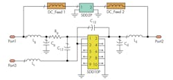
Figure 5 shows a novel SDD large-signal model of the HEMT. It mainly includes a SDD10P section, a SDD2P section, and other electrical components. The SDD10P portion is used to express the intrinsic region while external resistances, capacitances, and inductances are used to express the parasitic parameters, respectively. For high-frequency HEMT devices, it cannot be ignored that the coupling capacitance between the gate and drain (C12) and the coupling capacitance between the gate and source (C13) must accurately fit the high-frequency S-parameters.
This file type includes high resolution graphics and schematics when applicable.
Simplifying the Model
This file type includes high resolution graphics and schematics when applicable.
The source resistance (Rs) and drain resistance (Rd) are both deleted because the current between the source and drain in the SDD10P section can reflect the effect of these parameters, so that the large-signal model is simplified. All the parameters can be obtained through S-parameter fitting and optimization. Meanwhile, the SDD2P section compensates the DC characteristics by superposition with the SDD10P section. The two RF isolation inductances must be in series with the SDD2P section so that the RF characteristics cannot be affected. Therefore, the SDD large-signal model is complete and can satisfy the AlGaN/GaN HEMT’s DC and RF characteristics simultaneously.
The port parameters for the SDD10P are presented following Eq. 12. It should be noted that parameters Ids0, Cgs, Cgd, Cds, Ri, Rds,and τ represent the current between the source and drain, the capacitance between the gate and source, the capacitance between the gate and drain, the capacitance between the drain and source, the intrinsic channel resistance, the output resistance, and the delay time, respectively. Parameters Ids0, Cgs, and Cgd all change with changing Vgs and Vds in the model. The Statz nonlinear function model can be used to express their relationships according to Eq. 106:
In the linear region, 0 < Vds < 3/α:
In the saturation region, Vds ≥ 3/α:
where VTO, β, α, b, and λ represent the threshold voltage, the transconductance, the saturation voltage, the doping tailing factor, and the channel length modulation coefficient, respectively:
where Cgs0 and Cgd0 represent the capacitance between the gate and the source and the capacitance between the gate and the drain, respectively. Parameter δ is the fitting coefficient. For the SDD2P, the port parameters can be described as
I[1,0] = -Ids + Ids0 and
I[2,0] = Ids - Ids0
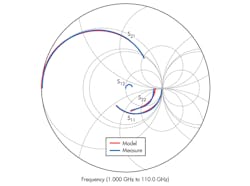
In this case, drain-source current Ids can express the DC characteristics accurately at different gate and drain voltages. It can still be obtained by using the Statz model. The S-parameters are shown in Fig. 6 by constructing the SDD large-signal model.
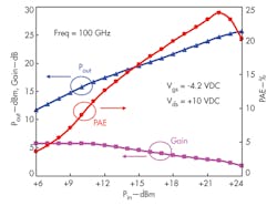
Figure 7 shows output characteristics of the HEMT device at 100 GHz with source and load-pull simulation. According to the maximum power gain match, the linear gain may reach 5.7 dB at small signal state until the input power is +11 dBm. The 1-dB compression point occurs when the input power rises to +15 dBm. The output power is close to +20 dBm and the power-added efficiency (PAE) may reach 16% to the 1-dB compression point. The PAE reaches its highest level when the input power is +22 dBm, a level of approximately 24%. In short, this HEMT represents a good device for higher-frequency monolithic-microwave integrated circuits (MMICs), especially for W-band applications.
This file type includes high resolution graphics and schematics when applicable.
Acknowledgments
This file type includes high resolution graphics and schematics when applicable.
This work was supported by the National Natural Science Foundation of China (No. 61306113) and the Beijing Higher Education Young Elite Teacher Project.
Luo Xiaobin, Doctor
Laboratory of Millimeter-Wave and Terahertz Technology, Beijing Institute of Technology, 100081, Beijing, China; e-mail:
Lv Yuanjie, Doctor
National Key Laboratory of Application Specific Integrated Circuit, Hebei Semiconductor Research Institute, 050051, Shijiazhuang, China
Yu Weihua, Professor
Laboratory of Millimeter-Wave and Terahertz Technology, Beijing Institute of Technology, 100081, Beijing, China
Lv Xin, Professor
Laboratory of Millimeter-Wave and Terahertz Technology, Beijing Institute of Technology, 100081, Beijing, China
Dun Shaobo, Doctor
National Key Laboratory of Application Specific Integrated Circuit, Hebei Semiconductor Research Institute, 050051, Shijiazhuang, China
Feng Zhihong, Researcher
National Key Laboratory of Application Specific Integrated Circuit, Hebei Semiconductor Research Institute, 050051, Shijiazhuang, China
References
1. R.S. Pengelly, S.M. Wood, J.W. Milligan, S.T. Sheppard, and W.L. Pribble, “A review of GaN on SiC high electron-mobility power transistors and MMICs,” IEEE Transactions on Microwave Theory & Techniques, Vol. 60, No. 6, June 2012, pp. 1764-1783.
2. S. Russo and A. Carlo, “Influence of the source–gate distance on the AlGaN/GaN HEMT performance,” IEEE Transactions on Electron Devices, Vol. 54, No. 5, May 2007, pp. 1071-1075.
3. F. Bernardini, V. Fiorentini, and D. Vanderbilt, “Spontaneous polarization and piezoelectric constants of III-V nitrides,” Physical Review B, Vol. 56, No. 16, October 1997, pp. R10024-7.
4. M. Farahmand, C. Garetto, E. Bellotti, K.F. Brennan, M. Goano, E. Ghillino, G. Ghione, J.D. Albrecht, and P.P. Ruden, “Monte Carlo simulation of electron transport in the III-nitride Wurtzite phase materials system: Binaries and Ternaries,” IEEE Transactions on Electron Devices, Vol. 48, No. 3, March 2001, pp. 535-542.
5. S.P. McAlister, J. A. Bardwell, S. Haffouz, and H. Tang, “Monitoring the self-heating in a high frequency GaN HFET,” Solid-State Electronics, Vol. 50, No. 6, June 2006, pp. 1046-1050.
6. H. Statz, P. Newman, and IRL. W. Smith, “GaAs FET device and circuit simulation in SPICE,” IEEE Transactions on Electron Devices, Vol. 34, No. 2, 1987, pp. 160-169.
This file type includes high resolution graphics and schematics when applicable.

Leaders relevant to this article:
