Transceiver ICs Energize Wideband Infrastructure
Wireless service providers face an ever-increasing demand for capacity on their networks, due to handheld devices that can process voice, data, and video. Not only must wireless infrastructure architects implement versatile systems using multiple data standards and frequency bands, but they must do so while occupying as little space and power as possible. To keep pace with the needs of infrastructure designers, Hittite Microwave Corp. has developed a new receiver and transmitter integrated-circuit (IC) chipset suitable for a wide range of cellular applications, from femtocells to macro base stations. The chipset features the model HMC1190LP6GE dual-channel downconverter, with integrated fractional-N phase-lock loop (PLL) synthesizer and voltage-controlled oscillator (VCO), for use with receivers. Also included is the model HMC1197LP7FE direct quadrature modulator, with fractional-N PLL frequency-synthesizer circuitry and VCO, for use with transmitters.
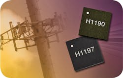
The two new ICs (Fig. 1) combine for efficient low-power operation over wide bandwidths, supporting a wide range of wireless communications standards. The HMC1190LP6GE downconverter IC, for example, covers an RF range of 700 to 3500 MHz, with typical power dissipation of only 2.34 W. But power consumption can be reduced further by means of external bias control pins, which allow high-speed optimization of power consumption under changing operating environments. This externally controlled enable/disable feature—combined with RF and external LO ports matched to 50 Ω—make it possible to dynamically reduce power consumption as conditions allow.
1. Model HMC1190LP6GE is a dual frequency downconverter with integrated VCO and synthesizer circuitry, while model HMC1197LP7FE is a direct modulator also with synthesizer and VCO circuitry.
With its integrated VCO and frequency-synthesizer circuitry, the HMC1190LP6GE is designed to provide excellent third-order-intercept (IP3) performance, as well as outstanding control of 2 x 2 spurious products. Unlike conventional narrowband frequency downconverters that are geared for only one or two wireless communications standards, the HMC1190LP6GE supports both high- and low-side LO frequency conversion plans across its full bandwidth. It incorporates a single-ended input port, with inputs converted to differential signals by means of an on-chip RF balanced-unbalanced (balun) circuit.
This approach allows for a variety of LO input/output (I/O) configurations, including a differential LO input for use with an external VCO and a differential LO output port. The latter allows a user to drive multiple receiver and transmitter frequency converters (as might be the case in some macrocells) using just a single HMC1190LP6GE dual downconverter IC. The HMC1190LP6GE’s RF input port and external LO input port are both matched to 50 Ω.
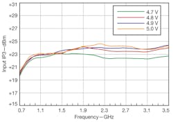
The HMC1190LP6GE incorporates a passive mixer core with high linearity and high-linearity intermediate-frequency (IF) amplifiers to achieve its excellent frequency-downconversion performance. It boasts RF-to-IF isolation of typically better than 45 dB, with LO leakage at the RF port of typically only -55 to -60 dBm. The 2 x 2 spurious products are controlled to -70 dBm, while channel-to-channel isolation of 50 dB on the downconverter help simplify filtering requirements. The dual downconverter delivers a wide dynamic range for a wide range of wireless standards. High input IP3 (IIP3) performance reaches +24 dBm for frequencies to 3500 MHz (Fig. 2). At the other end of the dynamic range, low noise figure of 9 dB enables the HMC1190LP6GE to contribute to excellent receiver sensitivity, meeting the most demanding wireless receiver applications.
2. This plot shows input IP3 performance as a function of frequency for the HMC1190LP6GE dual downconverter.
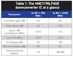
Additionally, the HMC1190LP6GE dual downconverter provides conversion gain that ranges from 6.2 dB at 2700 MHz to 8.4 dB at 900 MHz. It exhibits input 1-dB compression at power levels of +12 dBm at 2700 MHz and typically +10.7 dBm at 900 MHz. A summary of the dual downconverter’s performance can be found in Table 1.
The HMC1190LP6GE downconverter IC is ideal for diversity receivers in third-generation (3G) and fourth-generation (4G) cellular systems, as well as in multiple-input, multiple-output (MIMO) receiver architectures. Although it includes an internal VCO, its external VCO input port allows it to lock to external sources, enabling cascaded LO architectures for MIMO applications. Two separate charge-pump outputs enable separate loop filters optimized for both the integrated or external VCOs, with seamless switching possible between external and internal VCOs during operation for dynamically optimized performance. In addition, programmable RF output phase control makes possible phase adjustments and synchronization of multiple HMC1190LP6GE ICs in MIMO and phased-array beam-forming systems.
The HMC1190LP6GE downconverter provides a configurable LO output mute function and an “exact frequency mode” in which the IC’s fractional-N frequency synthesizer circuitry can be programmed to generate fractional frequencies with 0-Hz frequency error. Another powerful function is the capability to change frequencies without changing the phase of the output signal, which can greatly boost the efficiency of digital-predistortion (DPD) loops. The multifunction HMC1190LP6GE IC is housed in a RoHS compliant 6 x 6 mm leadless QFN package.
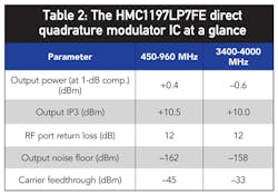
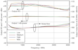
On the transmitter side, the model HMC1197LP7FE direct quadrature modulator also covers a broad frequency range, suitable for delivering digital modulation to wireless systems from 0.1 to 4.0 GHz [including 3G and 4G cellular, broadband wireless access (BWA), and Industrial-Scientific-Medical (ISM)-band applications]. Table 2 provides a sample of its performance. The low-noise direct modulator requires minimal external components and serves as a low-cost alternative to more complicated double-upconversion modulation approaches. Figure 3 highlights the wideband, high linearity performance of the HMC1197LP7FE. The highly integrated modulator/PLL/VCO delivers +10 dBm and better than +30 dBm output IP3 across all cellular infrastructure frequency bands from 400 to 4000 MHz. In addition, the low output noise floor (as low as -160 dBm/Hz) helps to maintain excellent signal-to-noise ratio for modulated signals.
3. The HMC1197LP7FE direct modulator IC features excellent dynamic range performance across its frequency range.
The single-ended RF output port is matched to 50 Ω with no external components, while the auxiliary LO output enables the HMC1197LP7FE to distribute identical frequency and phase signals to multiple destinations within a transmitter or receiver. An integrated programmable-bandwidth lowpass filter (LPF) in the LO path ensures little or no LO contribution to modulator sideband rejection. Sixteen programmable LPF bands enable true wideband operation, eliminating the need for band-specific harmonic filtering hardware and allowing agile LO frequency filtering for different band plans during and after deployment.
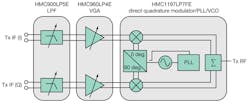
Figure 4 offers an example of how the HMC1197LP7FE direct modulator and various other ICs can be used to assemble a complete transmitter for cellular communications applications. Differential in-phase (I) and quadrature (Q) input signals are applied to the model HMC900LP5E baseband tunable lowpass filter and model HMC960LP4E digital variable gain amplifier (VGA) (both also from Hittite) to remove unwanted harmonic content, as well as to set I and Q signal strength. These differential signals are then fed to the HMC1197LP7E direct modulator, which requires only a power supply and crystal reference oscillator to then generate virtually any modulation format in any cellular frequency band.
4. This is an example of a wideband direct-conversion transmitter based on the HMC1197LP7FE direct modulator IC.
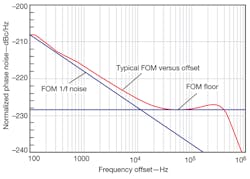
Figure 5 shows the PLL section common to both the HMC1190LP6GE downconverter and the HMC1197LP7FE modulator. The PLL section features a low figure-of-merit (FOM) noise floor of -227 dBm/Hz in fractional-frequency mode and -230 dBm/Hz in integer-frequency mode. The integrated root-mean-square (RMS) jitter is less than 150 fs. The modulator’s internal VCO circuitry can generate frequencies from 50 to 4100 MHz, while the PLL circuitry also accepts external VCO signals. This allows both the HMC1190LP6GE and the HMC1197LP7FE ICs to lock to external VCOs and enables cascaded LO architectures for MIMO radio applications.
5. This is a figure of merit versus frequency for the PLL/VCO section integrated into the HMC1190LP6GE and HMC1197LP7FE devices.
The PLL section’s integrated phase detector and delta-sigma modulator can operate to 100 MHz, permitting frequency synthesis with wide loop bandwidths and excellent spurious performance. In the HMC1197LP7FE modulator—as well as the HMC1190LP6GE downconverter—two separate charge-pump outputs enable separate loop filters for both the integrated and external VCOs, with seamless switching between internal and external VCOs. Also, the HMC1197LP7FE modulator, like the HMC1190LP6GE , can phase-adjust and synchronize multiple transmit and receiver ICs from Hittite for scalable MIMO and beam-forming architectures.
The PLL/VCO section in the HMC1197LP7FE shares the other features of the HMC1190LP6GE’s PLL/VCO section, including VCO mute control, synchronously changing frequency without changing phase, and the capability to generate fractional frequencies with 0-Hz frequency error. The HMC1197LP7FE direct modulator is housed in a compact 7 x 7 mm (LP7) surface mount QFN package.
The HMC1190LP6GE and the HMC1197LP7FE ICs feature stable performance over a wide temperature range, from -40 to +85°C. Their high levels of integration help simplify many wireless and cellular receiver and transmitter system designs at the infrastructure level, and their programmable power-consumption control helps “modulate” operating expenses for wireless base stations. In addition, with the broad frequency ranges covered by both of these ICs, one device can be used for a wide variety of different communications standards.
Hittite Microwave Corp., 2 Elizabeth Dr., Chelmsford, MA 01824; (978) 250-3333, FAX: (978) 2500-3373, www.hittite.com.
