Develop an Electronic Toll-Collection RSU Module with an RF Transceiver

What you’ll learn:
- How to implement a roadside module for electronic toll collection.
- Overview of the transmit and receive signal chains.
- A useful application of the module to test others like it in a production setting.
In 2019, electronic toll-collection (ETC) applications saw an explosion of growth in China due to government policy. The number of cars with installed on-board units (OBUs) increased from 80 million to 200 million in just one year. Along with this OBU installation boom, the use of ETC applications was extended from expressways to cities for things such as parking charges and vehicle-information collection.
Currently, the parking-charge and vehicle-information collection systems are camera-based. So, for ETC applications in urban settings, it’s desirable to integrate the ETC roadside unit (RSU) into the camera system.
This article describes an ETC RSU module implementation using a radio-frequency (RF) transceiver. Its target applications are China’s ETC RSUs, which means it must comply with the Chinese standard GB/T 20851-2019 “Electronic Toll Collection—Dedicated Short Range Communication.”1
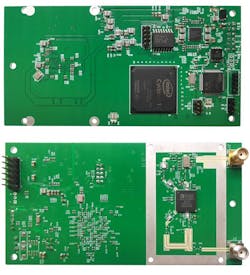
At just 11 × 6 cm, the module is very compact, so it’s easy to integrate with the camera system. What’s more, this ETC RSU module can be configured as a simple RF instrument, which could be used to test the ETC RSU module in a customer’s production line. Customers would not need an expensive RF instrument in their production line, resulting in huge cost savings.
Standard Summary
In keeping with the GB/T 20851-2019 standard, the ETC RSU physical-layer requirements are summarized in Tables 1 and 2.
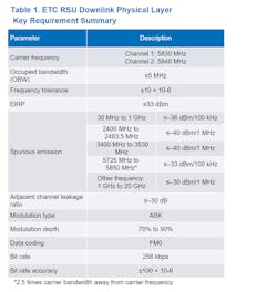
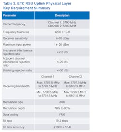
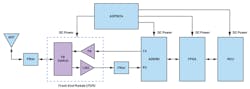
Figure 1 shows a block diagram for an ETC RSU module based on an RF transceiver, in this case the AD9361 from Analog Devices. The front view and back view of the module are shown in Figure 2.
This implementation can be configured for a wide range of applications. However, it’s well-suited for ETC RSU applications for several reasons.
First, in both the transmit and receive paths, the transceiver integrates programmable polyphase finite-impulse-response (FIR) filters that perform all digital-domain filtering inside the transceiver rather than in the FPGA. As a result, we save lots of FPGA resources and can choose a lower-cost FPGA. For example, to meet the receiving bandwidth requirement, engineers might use ADI’s Filter Wizard tool to design and tune the FIR filter response, and then get the filter coefficient to download into the AD9361 transceiver.
A transceiver with an integrated capacitor for the external crystal is also able to precisely tune and control the external crystal frequency. In a general implementation, developers adjust the RF phase-locked loop (PLL) N divider to meet the RF frequency tolerance requirement. However, this depends on the crystal’s performance to meet the bit-rate accuracy requirement, and it’s not adjustable.
Using digitally controlled crystal-oscillator (DXCO) capabilities allows the transceiver to tune the crystal frequency to meet the bit-rate accuracy and RF frequency tolerance at the same time. It’s also feasible to create a lookup table to compensate for any crystal frequency temperature drift, thus guaranteeing that the ETC RSU module meets the frequency tolerance and bit-rate accuracy requirement across the working temperature range.
Automatic gain control (AGC) also can be simplified when AGC functions are integrated in the transceiver. The AD9361, for example, implements two modes: slow AGC and fast AGC. These modes eliminate the need to implement any receiver gain-control function in the FPGA at all. The fast AGC mode is quite useful in ETC RSU applications, and it’s tested so that the gain adjustment settles down in the first few symbols of the uplink pilot signal.
The transmit path begins with the FPGA sending the transmitter digital-baseband signal to the transceiver. Inside the transceiver, that signal is filtered and interpolated from 10.24 to 163.84 Msamples/s. Next, the DACs convert the digital baseband signal into an analog baseband signal, after which it’s low-pass filtered.
That analog baseband signal is then upconverted to an RF signal at 5.83 GHz for Channel 1 or 5.84 GHz for Channel 2. In the transmitter RF domain, a transceiver with an attenuator can control the transmitter output power in a range greater than 80 dB. The attenuator is able to adjust the transmitter’s output-power level as well as gain temperature compensation for the whole transmitter link.
Next, the transmitter signal is fed into the power amplifier (PA) inside the front-end module (FEM). There, it’s further amplified and sent through a microstrip low-pass filter (LPF) to reject harmonics to meet the transmitter spurious emission requirement. Finally, the signal arrives at the antenna.
In our ETC RSU module design, the output power at the antenna port could reach 29 dBm with the AD9361’s transmitter attenuation set at 8 dB. Thus, the transceiver has enough attenuation dynamic range to compensate for both high-temperature gain decreases and low-temperature gain increases.
As to the receive path, the RF signal picked up by the antenna goes through the LPF. It’s then fed to the low-noise amplifier (LNA) inside the FEM, followed by a bandpass filter (BPF) to reject out-of-band interference signals.
Inside the transceiver receive path, the signal is further amplified and then downconverted to analog baseband. The analog baseband signal is low-pass filtered, and then the ADC converts it to a digital baseband signal. In the digital domain, the signal is filtered to meet the receiving bandwidth requirement and decimated from 163.84 to 10.24 Msamples/s. Subsequently, the transceiver sends the signal to the FPGA.
In this example, the module input voltage is 5 V. A quad buck regulator such as the ADP5014 can convert 5 V to 3.3 V, 2.5 V, 1.8 V, and 1.3 V. The 5-V input and four output voltages provide all of the voltage rails for the FEM, transceiver, FPGA, and MCU.
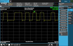
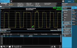
Transmitter Test Results
We tested all of the transmitter test cases defined in the standard, and the ETC RSU module passed the test with wide margins to spare. Screen captures of several key test cases are shown in Figures 3, 4, 5, and 6.
Receiver Test Results
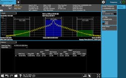
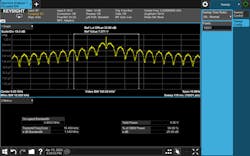
Likewise, we tested all of the receiver test cases defined in the standard, and as with the transmitter tests, the ETC RSU module easily passed. For the receiver sensitivity test, an FM0-coding, amplitude-shift-keying (ASK) modulated signal is downloaded into the signal generator. The demodulation algorithm is implemented inside the FPGA.
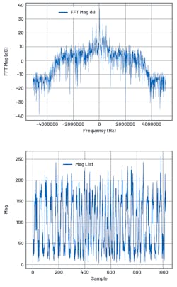
The ETC RSU module displays receiver sensitivity of –95 dBm, which is much better than the required –70 dBm. Figure 7 shows the I/Q-data FFT plot and the I/Q-data magnitude plot with an input signal of –95 dBm. Note that the signal still has quite good SNR when the input signal level is –95 dBm.
For other test cases, such as maximum input power, receiving bandwidth, in-channel interference rejection, adjacent channel interference rejection, and blocking rejection, the module passed all tests.
A Simple RF Instrument Implementation
This ETC RSU module could also be configured as a simple RF instrument to test ETC RSU modules and the antenna module in a production line. Because the transceiver has two RF channels, one channel can be used to implement the ETC RSU module while the other RF channel, together with an on-board, high-directivity microstrip coupler, can be applied to the return-loss test.
For the module transmitter test, one would use the transceiver’s receive signal strength indicator (RSSI) function. For example, the AD9361 transceiver’s RSSI function has 0.25-dB accuracy after calibration, which is good enough to test the ETC RSU module output power. Finally, for the module receiver test, the transceiver’s output power can be calibrated at one or two power levels. Then the transceiver’s internal attenuator could be used to provide a wide range of accurate output power to test the receiver.
Reference
1. GB/T 20851-2019 “Electronic Toll Collection—Dedicated Short Range Communication.”
About the Author
Tairan Sun
Product Applications Engineer, Analog Devices
Tairan Sun joined ADI Shanghai as a staff product-applications engineer in 2017. Before that, he was an algorithm engineer at DJI and an architecture engineer at ZTE. Tairan received a master’s degree of science in circuits and systems from Shanghai Jiao Tong University in 2012. He also received a bachelor’s degree of engineering in electronics and information engineering from Hefei University of Technology in 2009.
