Researchers Assess Thermal Conductivity, Defect Density of Four GaN Varieties
Semiconductors based on gallium-nitride (GaN) substrates are increasingly important in the power-device landscape. Their thermal conductivity, and thus their ability to conduct and so dissipate heat, is also a critical parameter.
A two-person team, based at the Nick Holonyak, Jr. Micro and Nanotechnology Laboratory at the University of Illinois at Urbana-Champaign, measured the thermal conductivity of four commonly used GaN substrate implementations along with other defining attributes. They noted that GaN thermal conductivity is reported to range from 110 to 269 W/m-K, which suggests a strong dependence not only on growth methods and conditions, but also measurement techniques and assumptions.
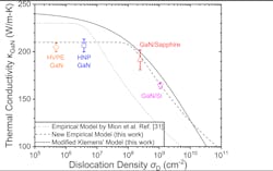
They noted that the standard thermal models as well as their relationship to dislocation densities may not be adequate given the different approaches (note that these dislocations adversely affect GaN-device performance). They anticipate that their new, presumably more-accurate model of the relationship between fabrication approach and the associated dislocation densities will lead to improved GaN process, thermal, and other models.
To do this, the researchers fabricated and tested four standard techniques used for fabricating c-plane GaN substrates, and measured their resultant thermal conductivity (κGaN) factors as follows:
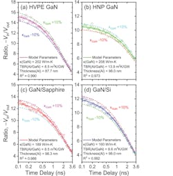
- 350-μm-thick freestanding GaN grown by hydride vapor phase epitaxy (HVPE): 204.7(±4.6) W/m-K
- 350-μm-thick freestanding GaN grown by high nitride pressure (HNP): 206.6 (±6.8) W/m-K
- 4.5-μm-thick GaN grown on the sapphire substrate by metal-organic chemical vapor phase deposition (MOCVD): 191.5 (±10.5) W/m-K;
- 5-μm-thick GaN grown on the Si(111) substrate by MOCVD with step-graded AlxGa1-xN, and AlN buffer layers in between: 164.4 (±3.2) W/m-K
To evaluate the thermal conductivity, they employed standard time-domain thermoreflectance (TDTR) techniques with a laser light source generating pulses at an 80-MHz repetition rate. These pulses were split into a pump beam and a probe beam, with the pump beam modulated by an electro-optical modulator using a 200-Hz chopper. A fast-response photodiode detector coupled with an RF lock-in amplifier was then used to pick up the reflected laser signal. The resulting graphs also show the time delay (in seconds) used to allow the thermal energy to propagate through the sample (Fig. 1).
Their efforts didn’t end with the measurement of thermal conductivity. In addition, they used sophisticated cathodoluminescence (CL) and X-ray diffraction techniques to evaluate crystal dislocation densities (σD) along with secondary ion mass spectroscopy to measure impurity concentration. Finally, they developed a complex empirical model equating the relationship between thermal conductivity and these dislocation densities, and believe it explains the experimentally observed rate of decrease in κGaN with increasing σD (Fig. 2).
The team further believes their work shows that the thermal conductivity of a heteroepitaxially-grown GaN material can be estimated based on its dislocation densities, thus providing key design guidelines for thermal management in these semiconductor devices. The device-fabrication physics study, which was supported by the Air Force Office of Scientific Research (AFOSR), is published as “Impact of dislocations on the thermal conductivity of gallium nitride studied by time-domain thermoreflectance” in the Journal of Applied Physics from the American Institute of Physics, with additional Supplementary Online Material as well.
About the Author

Bill Schweber
Contributing Editor
Bill Schweber is an electronics engineer who has written three textbooks on electronic communications systems, as well as hundreds of technical articles, opinion columns, and product features. In past roles, he worked as a technical website manager for multiple topic-specific sites for EE Times, as well as both the Executive Editor and Analog Editor at EDN.
At Analog Devices Inc., Bill was in marketing communications (public relations). As a result, he has been on both sides of the technical PR function, presenting company products, stories, and messages to the media and also as the recipient of these.
Prior to the MarCom role at Analog, Bill was associate editor of their respected technical journal and worked in their product marketing and applications engineering groups. Before those roles, he was at Instron Corp., doing hands-on analog- and power-circuit design and systems integration for materials-testing machine controls.
Bill has an MSEE (Univ. of Mass) and BSEE (Columbia Univ.), is a Registered Professional Engineer, and holds an Advanced Class amateur radio license. He has also planned, written, and presented online courses on a variety of engineering topics, including MOSFET basics, ADC selection, and driving LEDs.
