Develop a BPF from a Compact DGS LPF
This file type includes high-resolution graphics and schematics when applicable.
Wave propagation in periodic structures has been studied for some time as part of applied physics investigations.1,2 Recently, periodic structures, such as photonic-bandgap (PBG) structures and defected ground structures (DGS) for planar transmission lines, have drawn wide interest in applications for microstrip filters, antennas, and millimeter-wave circuits.
A DGS is realized by etching away a defected pattern from a circuit ground plane. 3-12 The etched defect disturbs the shield current distribution in the ground plane. This disturbance can change transmission-line characteristics, such as line capacitance (C) and inductance (L), possibly giving rise to the effective C and L of a transmission line, respectively. Thus, an LC equivalent circuit can be used to model the proposed DGS loop circuit. A C-shaped loop resonator consists of two arms—a short continuous arm and a long arm with a gap (g) near the middle. Simple relations will be used to obtain the equivalent-circuit parameters utilizing the simulation response of the DGS.13-16
To explore the capabilities in lowpass filters (LPFs) and bandpass filters (BPFs), DGS design methods were employed with the aid of commercial computer simulations. The first filter design, a compact multilayer LPF, employs a single suspended C-shaped open-loop resonator. The second filter, a BPF, is extracted from the first, adding a feed-discontinuity, in-state-compensated patch capacitor. Both filters feature compact size, high sharpness factor, wide stopband response, and flexibility in design. Measured S-parameters indicate high performance levels, with good agreement between simulations and measurements.
Leveraging the Bandstop Filter
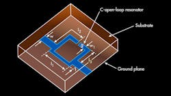
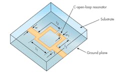
The building block of a proposed LPF is a C-shaped open-loop bandstop filter; it employs a single microstrip stepped open-loop resonator that is directly connected with two feed lines (Fig. 1). The high-impedance line between the two feed lines has a constant width corresponding to an impedance of 75 â¦. The bandstop filter was designed at a center frequency of around 5.6 GHz, and simulated and fabricated on circuit material with relative dielectric constant (εr) of 3.38 and thickness of 0.813 mm.
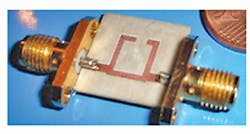
The dimensions of the proposed filter are as follows: l1 = 8 mm, l2 = 7.6 mm, l3 = 4.08 mm, w = 1.92 mm, w1 = 1 mm, g = 1 mm, and t = 2 mm. The two feed lines have a characteristic impedance of 50 â¦. Fig. 2 shows the fabricated cell (a single bandstop filter).
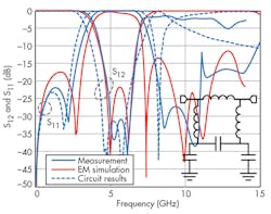
The results of electromagnetic (EM) simulation, equivalent-circuit simulation, and measurements are shown in Fig. 3. Good agreement among them demonstrates the validity of the equivalent-circuit model for the proposed bandstop filter. The insertion loss is less than 0.5 dB from dc to 3 GHz, while the return loss is less than -22 dB in the passband. The stopband rejection levels are more than 20 dB from 4.7 to 6.7 GHz. The proposed filter exhibits a sharp cutoff, dropping from less than -0.5 dB to almost -44 dB within 1.5 GHz. The proposed bandstop filter measures 7 × 7 mm2(Fig. 2, again).
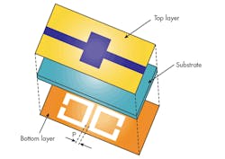
Designing a LPF with large reject band and high transition domain, based on a C-shaped, open-loop DGS cell required the use of two cascaded C-shaped open-loop DGS resonators (Fig. 4). This LPF consists of one compensated microstrip line on the top layer and two coupled C-DGS slots. Both C-DGS slots are etched next to each other on the metallic ground plane of a printed circuit board (PCB). The close proximity results in electric coupling between the resonators.
To verify the response of the proposed microstrip LPF, a simple structure was simulated and optimized on RO4003 circuit material from Rogers Corp., with thickness of 0.815 mm and εr of 3.38 (Fig. 4, again). The LPF was designed with a cutoff frequency of 3.5 GHz and passband insertion loss of less than 0.3 dB. It has a transmission zero near the passband edge at 4.1 GHz, which gives a very sharp slope (S) response in the transition domain. This filter also has a wide rejection band, to 7.5 GHz.
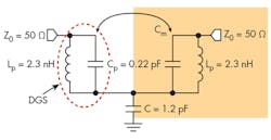
The width of the microstrip line was chosen to be 1.9 mm for a characteristic impedance (Z0) of 50 â¦. Other structural parameters are: p = 4 mm, a = 4 mm, and b = 8 mm. The proposed LPF structure was simulated via equivalent-circuit model (Fig. 5) in a commercial software circuit simulator.
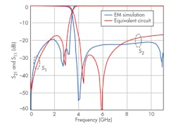
The top compensated open-stub capacitor is connected to both 50-⦠feed lines. Fig. 6 provides a comparison between EM and equivalent-circuit simulations of the LPF. As can be seen, the circuit model simulation agrees closely with the EM simulation results except at the attenuation pole frequency. The main reason for the discrepancy is an ideal model has been adopted in circuit simulation and for the substrate without accounting for radiation. The equivalent circuit corresponding to the proposed DGS can be extracted by S-parameters and Eq. 1 for capacitor Cp and inductor Lp:
C p = (1/200)[ fcπ(f 20 – f2c)] F
Lp = [ 0.25/C(πf0)2H] (1)
The corresponding equivalent-circuit model for a three-pole LPF was developed to account for the mutual coupling between the DGS slots. A three-pole stub-type LPF with DGS slot was adapted from a reference source.
As is well known, coupling depends on the distance between resonators, as well as from the attenuation pole location, which corresponds to the resonance frequency. The coupling between the two resonators can be used to improve the filter characteristics, particularly the rejection bandwidth. However, it is not always simple to define the ideal coupling distance.
For the current design, the effective distance between the two resonators (p) = 3 mm, which is the value of the coupling coefficient between two DGS resonators, was determined through a MATLAB (from MathWorks) interpolation program and using an empirical method. The use of two coupled DGS C-shaped resonators combined with a top patch compensated capacitor facilitates the design of a wide-rejection-band LPF (Fig. 6, again):
fe = 1/2π (cp + cm)0.5Lp
fm = 1/2π (cp – cm)0.5Lp (2)
KM
= (f2/fe – f2/f m)/ (f2/f e + f2/f m)
= Cm/Cp (3)
The LPF was designed and fabricated on a 0.813-mm-thick commercial circuit laminate with εr of 3.38 (Rogers RO4003). The value of coupling coefficient p was extracted using the Microwave Office full-wave EM simulator from AWR Corp. and MATLAB mathematical analysis software.
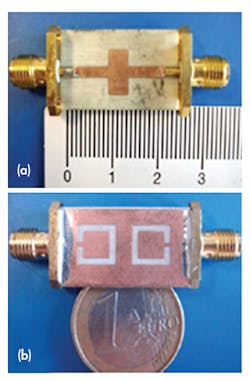
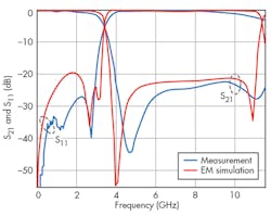
The simulated and measured results show that the passband insertion loss is less than 0.1 dB over the whole passband, and the attenuation level is less than -20 dB within a very broad stopband to about 8 GHz. Fig. 7 shows the fabricated microstrip filter with uniform metal-loaded slots etched in the ground plane, while Fig. 8 compares measured and simulated results, which are in good agreement. The filter achieves wide stopband, sharp transition band, and enhanced passband performance.
From LPF to BPF
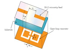
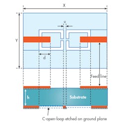
To realize the transformation of the LPF to BPF without using additional components, a J-inverter gap is etched in the middle of the 50-⦠feed line on in the top layer of the conventional structure (Fig. 9). The proposed structure consists of two open-loop C-shaped resonators, which are etched in the ground plane. Placement of the two DGS elements ensures that they have magnetic coupling rather than electric coupling as before.
The modified structure is similar to the cascaded filter described earlier, with a simple modification to the exciting feed line on the upper layer (Fig. 9, again). This DGS topology has been found to improve filter performance while significantly reducing the total size of the structure. The gap distance (q) between both microstrip feed lines can be defined by either the coupling matrix method or empirical method.
By using the coupling matrix method, the coupling spacing can be exactly calculated. The disadvantage of this method is the complicated way to define the required values. The empirical process is simpler, but the disadvantages are the long duration of the process and inaccurate results.
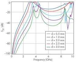
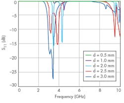
The filter was simulated on a substrate with a relative dielectric constant of 3.38 and thickness of 0.813 mm. With consideration of d, several simulation results of this filter are shown in Fig. 10. To study the features of this structure, different investigations were carried out on gap length. As Fig. 10 shows, if p and g are fixed and, at the same time, d is varied, passband frequency and insertion loss can be controlled. This means that the gap length significantly affects the insertion loss, as well as the quality factor Q and rejection band of the structure.
In the second step, d and g are fixed, while the effects of variations in u are studied empirically. The dimensions of the extracted filter shown in Fig. 9 are g = 1 mm, u = 1 mm, d = 0.5 to 3.0 mm, and q = 5 mm. The DGS BPF was simulated using Microwave Office software. Simulation results are given in Fig. 10, which shows the characteristics of a bandpass filter with wireless-local-area-network (WLAN) features. At d = 2.5 mm, the filter has a 3-dB cutoff frequency (fc) and resonance frequency (f0) of 3.0 and 3.65 GHz, respectively.
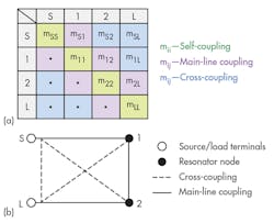
A coupling matrix method was used to improve the performance of the previously described BPF illustrated in Figs. 9 and 10. Fig. 11 shows the topology of the N × N matrix assembling the values of the mutual couplings between the nodes of the network. There are three variations to consider:
1. If the coupling is between sequentially numbered nodes (M j, j+1), it is referred to as a direct coupling.
2. The elements, which are placed on the main diagonal (M j, j) are self-coupling.
3. The other remaining couplings between the nonsequentially numbered nodes are known as cross-couplings.
Because of the reciprocity of the passive network, M i, j = M j, i, the matrix symmetrical about the main diagonal and generally all entries may approach zero, but remain nonzero. Any additional resonator or variation in the coupling values with frequency (dispersion) can lead to a change of the coupling-matrix structure.
The n + 2 normalized coupling matrix (M) provides a full description of all coupling paths in a filter, where n + 2 is the order of the matrix M and n is the filter order. All elements of the symmetrical matrix M will be designated as mij = mji. The input and output connections are included, thus the n + 2 coupling matrix is extended. This extension corresponds to the “+2” term. Fig. 5 explains the n + 2 coupling matrix in more detail for the folded topology.
To realize a coupling matrix, which conforms to a chosen topology, it is necessary to give first the specifications of the filter. The desired parameters will subsequently be extracted by using an optimization-based scheme.17, 18 The coupling coefficient and quality factor curves19, 20 are then used to realize the obtained coupling coefficients. In our case, the second-order filter is with a bandwidth BW = 1 GHz, return loss RL = 20 dB, and center frequency f0 = 3.3 GHz. The coupling matrix obtained from the optimization scheme is:
and the external quality factors are q1 = q2 = 0.9136. Using the (denormalized) coupling matrix (M), external quality factors (qi), and normalized coupling matrix and scaled quality factors Qi, the required fractional bandwidth (FBW), the actual (denormalized) coupling matrix, and the scaled external Q can be calculated by Eqs. 5-9:
BW = f2 - f1 (5)
FBW = BW/f0 = 30.3% (6)
m = FBW × M (7)
Qi = qi /FWB (9)
Based on these calculated values of the coupling coefficients mij and using the coupling coefficients curve, the coupling distance was selected as u = 0.75 mm.
As has been shown in earlier works,17-20 the external Q can be easily determined through f – 90°, f + 90°, and center frequency f0, as well as the relationship (empirical curve)
between the external quality factor (Qi), with i = 1, 2, and coupling distance (d). Using the coupling curve, the optimal value for Qi leads to a value of coupling distance d. In this case, Q1 = Q2 = 3 and d = 2.8 mm (Fig. 12).
Figure 12 shows two-dimensional (2D) views of the proposed bandpass filter. The coupling distance between the cascaded DGS resonators (u) and the coupling distance between the feed and the first DGS resonator (d) can be seen in Figs. 9 and 12. To verify the performance and the efficiency of the filter, the structure was designed, simulated, and optimized. Fig. 12 shows a design of the DGS bandpass filter. The total area of the filter is:
(0.202λg × 0.101λ g
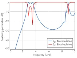
where λg = 49.5 mm. The simulation results of the optimized bandpass filter are located in the frequency range from dc to 8 GHz as shown in Fig. 13. Using the coupling matrix method, an improved BPF has been achieved by extraction from the LPF. The bandpass filter has sharp edge steepness in its passband-stopband transition regions. The useful signal’s second unwanted harmonics at twice the center frequency is suppressed, leading to a large reject band until under -20 dB to 4 GHz.
Acknowledgments
The author wishes to thank the German Research Foundation (DFG) for financial support. The author also thanks M. Sc. Eng. Sonja Boutejdar, Mehdi Boutejdar, and Karim Boutejdar for their assistance and help, and Mr. Harald Dempewolf, the Laboratory Manager of the Institute for Electronics, Signal Processing, and Communication (IIKT) at the University of Magdeburg, Germany, for his support.
Ahmed Boutejdar is Doctor-Scientist Researcher at the German Research Foundation (DFG)-Braunschweig-Bonn, Electrical Engineering, Braunschweig-Bonn, Germany; e-mail: [email protected].
References:
1. D. Sridhar Raja, “Periodic EBG Structure Based UWB Band Pass Filter,” International Journal of Advanced Research in Electrical, Electronics and Instrumentation Engineering Vol. 2, No. 5, May 2013.
2. Shao Ying Huang and Yee Hui Lee, “Tapered Dual-Plane Compact Electromagnetic Bandgap Microstrip Filter Structures,” IEEE Transactions on Microwave Theory & Techniques, Vol. 53, No. 9, September 2005.
3. Ahmed Boutejdar, A. Elsherbini, and A.S. Omar, “A Compact Microstrip Multi-Layer Lowpass Filter Using Triangle Slots Etched in the Ground Plane,” Proceedings of the 36th European Microwave Conference 2006 (EuMC), Manchester, UK, September 2006.
4. Mohamed Awida, Ahmed Boutejdar, Amr Safwat, Hadia El-Hannawy, and A. Omar, “Multi-Bandpass Filters Using Multi-Armed Split Ring Resonators with Direct Feed,” Proceedings of the IEEE MTT-S International Microwave Symposium (IMS), Honolulu, HI, June 2007.
5. J.-S. Lim, Ch.-S. Kim, Y.-T. Lee, et al., “A new type of lowpass filter with defected ground structure,” European Microwave Week, Milan, Italy, September 24-26, 2002.
6. A. Boutejdar, A. Elsherbiny, and A.S. Omar (Invited), “A Novel Method to Obtain a Large Reject Band with a Compact Bandstop Filter Using Detected Ground Structure (DGS) Coupled Resonators,” Mediterranean Microwave Symposium Genova, Italy, September, 2002.
7. D. Ahn, J. Park, C. Kim, Y. Qian, and T. Itoh, “A Design of the Lowpass Filter Using the Novel Microstrip Defected Ground Structure,” IEEE Transactions on Microwave Theory & Techniques, Vol. 49, No. 1, January 2001, pp. 86-93.
8. A. Boutejdar, “A New approach to Design Compact Tunable BPF Starting from Simple LPF Topology Using a Single T-DGS-Resonator and Ceramic Capacitors,” Microwave and Optical Technology Letters, Vol. 58, No. 5, May 2016, pp. 1142-1148.
9. H. Liu, X. Sun, and Z. Li, “Novel two-dimensional (2D) defected ground array for planar circuits,” Active and Passive Electronic Components, Vol. 27, No. 3, 2004, pp. 161-167.
10. Ahmed Boutejdar, W. Abd Ellatif, A. A. Ibrahim, and M. Challal, “A simple transformation from lowpass to bandpass filter using a new quasi-arrow head defected ground structure resonator and gap-J-inverter,” Microwave and Optical Technology Letters, Vol. 58, No. 4, April 2016, pp. 947-953.
11. Z. Pan and J. Wang, “Design of the UWB bandpass filter by coupled microstrip lines with U-shaped defected ground structure,” in Proceedings of the International Conference on Microwave and Millimeter Wave Technology (ICMMT ’08), Vol. 1, April 2008, pp. 329-332.
12. H. Liu, B. Ren, X. Xiao, Z. Zhang, S. Li, and S. Peng, “Harmonic-rejection
compact bandpass filter using defected ground structure for GPS application,” Active and Passive Electronic Components, Vol. 2014, Article ID 436964, 2014, 4 pages.
13. Ahmed Boutejdar, “Design of broad-stop band low pass filter using a novel quasi-Yagi-DGS-resonators and metal box-technique,” Microwave and Optical Technology Letters, Vol. 56, No. 3, March 2014, pp. 523-528.
14. Ahmed Boutejdar, Ahmed A. Ibrahim, and Edmund P. Burte, “Design of a Novel Ultrawide Stopband Lowpass Filter Using a DMS-DGS Technique for Radar Applications,” International Journal of Microwave Science and Technology, Vol. 2015 (2015), Article ID 101602, 7 pages.
15. A. Boutejdar, A.Omar, and E. Burte, “LPF builds on quasi-Yagi DGS,” Microwaves & RF, Vol. 52, No. 9, September 2013, pp. 72-77.
16. A. Boutejdar and A. Omar, “Compensating For DGS Filter Loss,” Microwaves & RF, Vol. 51, No. 9, February 2012, pp. 68-76.
17. J.S. Hong and M. J. Lancaster, Microstrip Filters for RF/Microwave Applications, John Wiley & Sons, New York, 2001.
18. Richard J. Cameron, “Advanced Coupling Matrix Synthesis Techniques for Microwave Filters,” IEEE Transactions on Microwave Theory & Techniques, Vol. 51, No. 1, January 2003.
19. Ahmed Boutejdar, “Design of 5 GHz compact reconfigurable DGS bandpass filter using varactor-diode device and coupling matrix technique,” Microwave and Optical Technology Letters, Vol. 58, No. 2, February 2016, pp. 304-309.
20. Ahmed Boutejdar, Theme der Ph. D. thesis: “Entwurf, Entwicklung und Optimierung von kompakten HF-Mikrostreifen-Filtern mittels Defected Ground Structure-Technik (DGS)” doctorate degree (Dr. Eng.). At Ottovon-Guericke University, Magdeburg, November 2010.
