CCCDTAs Form Flexible Biquad Filter
This file type includes high resolution graphics and schematics when applicable.
Filters have long been instrumental in cleaning and sorting signals. Likewise, the concept of a “universal” filter has long intrigued designers in search of flexible signal-processing solutions. In quest of that universal filter, which is a circuit that can realize all basic filtering functions, a transadmittance-mode (TA-M) universal biquad filter has been developed based on current-controlled, current-differencing transconductance amplifiers (CCCDTAs).
In a configuration with two CCCDTAs, two capacitors, and no resistors, this filter can realize all standard filtering functions. Among these are lowpass-filter (LPF), highpass-filter (HPF), bandpass-filter (BPF), bandstop-filter (BSF), and even all-pass filter (APF) responses using the same circuit structure. The design also offers great convenience, via electronic tuning of center frequency, quality factor (Q), and bandwidth. The TA gains of LPF, BPF, and HPF functions can be independently and electronically adjusted by means of bias currents to the CCDTAs. Since the CCCDTAs exhibit high input and output impedances, this flexible filter does not require impedance matching when cascaded with other circuits.
Analog filters have long been essential building blocks for electronic design.1,2 In recent years, a variety of current-mode (CM) and voltage-mode (VM) filter circuits have been developed with active devices, such as operational transconductance amplifiers (OTAs), current conveyors (CCs), and current differencing transconductance amplifiers (CDTAs). In many electronic systems, the use of voltage-to-current interface circuits is essential, since CM and VM circuits in these systems must be connected. In the process of making these voltage-to-current interfaces, it is also possible to realize signal processing, such as filtering, and the TA-M filter is a tremendous boost for these situations.3
A number of TA-M filter studies have been published.3-14 Unfortunately, all of these design efforts suffer from various shortcomings, including an overabundance of passive elements (notably resistors); lacking the capability to realize all standard filtering functions; lacking the capability to be controlled electronically; not being able to tune the gain of LPF, BPF, and HPF functions independently and electronically; low input and output impedance; and the lack of need for an element matching condition.
Since a novel active-element design was first reported as a CCCDTA,15 a wide range of CCCDTA-based applications have been realized.15-24 The present design offers simplicity, electronic tenability, and high output impedance for versatility. Its parasitic resistance at two current input ports can be controlled by input bias current. As a result, in some circuit designs, there is no need for additional resistors to create an integrator circuit.
By exploring the capabilities of these CCCDTA designs, it was possible to create a novel TA-M universal biquad filter using CCCDTAs. The proposed circuit employs two CCCDTAs and two capacitors, one of which is permanently grounded. The circuit topology is suitable for integrated circuit (IC) fabrication. With its three voltage input terminals and single current output terminal, the circuit can realize all standard filtering functions. Key parameters can be controlled by adjusting different bias currents for the CCCDTA.
The new CCCDTA design has been simulated with commercial software, and the simulations agree closely with theoretical analysis of the design. The table presents a comparison of the new design with previously published TA-M filters. This new design approach reduces the number of active and passive circuit elements required and overcomes some of the limitations of the earlier designs.
This file type includes high resolution graphics and schematics when applicable.
Deconstructing the CCDTA
This file type includes high resolution graphics and schematics when applicable.
In general, a CCDTA can be represented by the diagram of Fig. 1(a) and the equivalent circuit of Fig. 1(b). The matrix of Eq. 1 portrays the CCCDTA’s terminal relationships:
where:
p and n = positive and negative current input terminals with finite resistances Rp and Rn, respectively, at those terminals;
z and x = current output terminals, which have high output impedance;
gm = the transconductance gain, which can be tuned by using the external bias current of the CCCDTA;
VZ = the voltage drop at terminal Z, which is turned into a current output by means of a transconductance stage.
Figure 2 presents a realization of a proposed CCCDTA universal filter.24 The circuit is comprised of a current-controlled current differencer and a multiple-output operational transconductance amplifier (MO-OTA). The current-controlled current differencer consists of bipolar transistors Q1 through Q42. Bipolar transistors Q43 through Q54 form an MO-OTA, which is composed of transconductance circuits and multiple-output current mirror circuits. The transconductance gain and input resistance at two current input terminals (the p and n ports) can be directly controlled by the diverse bias currents of the CCCDTA, allowing for flexibility and versatility in many different applications.
In this CCCDTA design, resistances Rp and Rn and transconductance gm can be expressed by means of Eqs. 2-4:
where:
VT = the thermal voltage;
IB1, IB2, and IB3 = the bias currents of the CCCDTA, which are used to control the intrinsic resistances and transconductance of the filter.
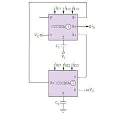
Figure 3 shows a circuit diagram of the designed transadmittance filter. From the diagram, it can be seen that a TA-M universal filter is relatively easy to realize by adopting minimum active and passive elements for the design. With its resistorless configuration, the filter design is also quite suitable for monolithic integration. Using Eqs. 1-4, the characteristic equations of Fig. 3 are:
where:
Rin = the finite negative input resistance of the CCCDTA, and
Rip = the finite positive input resistance of the CCCDTA.
By analysis of Fig. 3 and Eqs. 5 and 6, the five current-transfer functions for the LPF, BPF, HPF, BSF, and APF responses can be obtained in the following ways. The LPF response can be achieved by means of Eq. 7 when V3 = Vin and V1 = V2 = 0:
The BPF response can be achieved by means of Eq. 8 when V2 = Vin and V1 = V3 = 0:
The HPF function can be achieved with the aid of Eq. 9, when V1 = Vin and V2 = V3 = 0:
The BSF response can be gained with the help of Eq. 10 and when IB12 = IB13 and when V1 = V3 = Vin:
The APF response can be achieved with the help of Eq. 11 and when IB12 = IB13= IB21 and when V1 = V2 = V3 = Vin:
This file type includes high resolution graphics and schematics when applicable.
Delving Deeper
This file type includes high resolution graphics and schematics when applicable.
From Eqs. 7-11, it is evident that Fig. 3 provides second-order LPF, BPF, HPF, BSF, and APF responses from the same circuit design through the selection of different input signals. It is also apparent that there is no need for an external inverter and a matching element to realize BS and AP filters. The parameters of ω0, Q, and ω0/Q (bandwidth) for the proposed filter can be found from Eqs. 12-14:
From Eqs. 12-14, it is clear that all the characteristic parameters of this filter can be electronically tuned by CCCDTA bias currents. Also, ω0 and Q can be adjusted electronically and independently by means of IB23 without obstructing the value of ω0/Q.
By using Eqs. 7-9, the transadmittance gain of the LPF, BPF, and HPF responses can be calculated by means of Eqs. 15, 16, and 17, respectively:
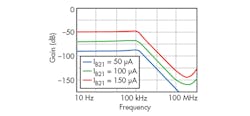
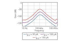
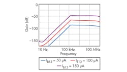
From these three expressions, it is easy to see that the transadmittance gains of the LP, BP, and HP filter functions can be independently and electronically modified by adjusting the different bias currents: IB21, IB12, and IB13. The lowpass and bandpass gains—GLP and GBP, respectively—can be independently transformed by means of bias currents IB21 and IB12, respectively, without the poly-frequency and bandwidth of the particular filter response.
Considering the CCCDTA’s nonideal characteristics, its port relationship in Fig. 3 can be rewritten as Eq. 18:
where:
αpi (αpi = 1 - εpi, |εpi| << 1) and αni (αni = 1 - εni, |εni| << 1)
are parasitic current gains between p → z and n → z terminals of the ith CCCDTA, respectively, and
βi (βi = 1 - εi, |εi| << 1)
is the parasitic transconductance tracking error from the z to the x terminals.
The circuit in Fig. 3 was reanalyzed by using Eq. 18, and the modified current transfer characteristic is approximated by Eq. 19:
From Eq. 19, the nonideal values of ω0 and Q for the universal filter can be expressed by means of Eqs. 20 and 21, respectively:
The sensitivities of the active and passive components to ω0 can be found by means of Eqs. 22 and 23:
It can be noted from Eqs. 22 and 23 that all sensitivities of the passive and active elements of the proposed TA-M filter do not exceed 50% in magnitude.
It was possible to simulate a TA-M filter as portrayed in Fig. 3 by using the CCCDTA in Fig. 2 simulated with the parameters of the PR200N and NR200N bipolar transistors of the ALA400 transistor array from AT&T in a PSPICE simulator.25 The power supplies were set as VDD = -VSS = 1.5 V.
This file type includes high resolution graphics and schematics when applicable.
Summing Up
This file type includes high resolution graphics and schematics when applicable.
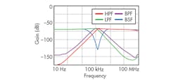
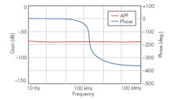
The universal filter was designed using passive component values of C1 = C2 = 1 nF. Bias currents for the CCCDTAs were chosen as IB11= IB22 = 500 μA (for R1p = R2n = 20 Ω); IB12 = IB21= 100 μA; and IB13 = IB23 = 100 μA (for gm = 1.2 mS). Using Eq. 12, a polyfrequency of 190 kHz was achieved through these values. By selecting different input signals, it was possible to achieve simulated responses for LPF, BPF, HPF, and BSF functions (Fig. 4). Figure 5 offers simulated responses for the gain and phase of the APF function.
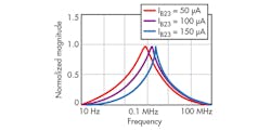
From Figs. 4 and 5, it is apparent that the proposed TA-M filter circuit can realize LP, HP, BP, BS, and AP functions depending upon input signal selection, without modifying the basic circuit framework. By setting different IB23 values, the different BPF magnitude responses of Fig. 6 can be achieved. It is clear that the polyfrequency and Q of the filter can be adjusted electronically. The electronic tuning of gain for LPF, BPF, and HPF responses are achieved by changing bias currents from 50 to 150 μA while maintaining C1 = C2 = 1 nF, as shown in Figs. 7 through 9.
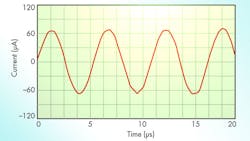
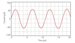
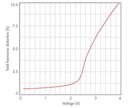
To test the large-signal behavior of the TA-M filter, a sinusoidal input at 190 kHz and 0.5 V was applied to the APF function with the active and passive circuit elements as established previously. Figure 10 shows the results of the output transient response, while the total harmonic distortion (THD) is presented in Fig. 11. For an input signal of less than 2.5 V, the TA-M filter’s THD is less than 3.5%.
In short, this is a single circuit that can be electronically tuned for different filter responses, and it can realize all standard filtering functions. Being completely without resistors, it is well suited for IC fabrication. It is a versatile design that is well suited for a wide range of applications, including in communications and electronic control systems and circuits.
Acknowledgments
The authors would like to thank the reviewers for their valuable comments and helpful suggestions. This work is supported by the foundation of outstanding youth science and technology innovation team of the Hubei Polytechnic University (No. 13xtx02) and the project planning of young teachers in enterprises of the Hubei Province (No. XD2014681), both of the People’s Republic of China (PRC).
Shaojiang Lin, Professor
Qinian Shi, Professor
School of Mechanical and Electrical Engineering, Hubei Polytechnic University, Huangshi 435003, People’s Republic of China
References
1. G. Triantafyllou, I. Hoteit, and X. Luo, “Assessing a robust ensemble-based Kalman filter for efficient ecosystem data assimilation of the Cretan Sea,” Journal of Marine Systems, Vol. 125, 2013, pp. 90-100.
2. J. Jin, “Resistorless Active SIMO Universal Filter and Four Phase Quadrature Oscillator,” Arabian Journal for Science and Engineering, 2014, pp.1-8.
3. A. Toker, O. Cicekoglu, S. Ozcan, and H. Kuntman, “High-output-impedance transadmittance type continuous-time multifunction filter with minimum active elements,” International Journal of Electronics, Vol. 88, 2001, pp.1085-1091.
4. U. Cam, “A new transadmittance type first-order allpass filter employing single third generation current conveyor,” Analog Integrated Circuits and Signal Processing, Vol. 43, 2005, pp. 97-99.
5. S.K. Paul, N. Pandey, and A. Bhattacharyya, “Transadmittance mode universal filter based on MOCCCII[C],” CODEC 2009, 4th International IEEE Conference on Computers and Devices for Communications, 2009, pp. 1-4.
6. N. Pandey and S.K. Paul, “SIMO Transadmittance Mode Active-C Universal Filter,” Journal of Circuits and Systems, Vol. 1, 2010, p. 54.
7. N.A. Shah, S.Z. Iqbal, and B. Parveen, “SITO high output impedance transadmittance filter using FTFNs,” Analog Integrated Circuits and Signal Processing, Vol. 40, 2004, pp. 87-89.
8. N.A. Shah, M. Quadri, and S.Z. Iqbal, “CDTA based universal transadmittance filter,” Journal of Analog Integrated Circuits and Signal Processing, Vol. 52, Nos. 1-2, 2007, pp. 65-69.
9. N.A. Shah, S.Z. Iqbal, and B. Parveen, “Lowpass and bandpass transadmittance filter using operational amplifier pole,” AEU International Journal of Electronics and Communication, Vol. 59, 2005, pp. 410-412.
10. M.A. Brahim and H.A. Kuntman, “A Novel Transadmittance-Type KHN-Biquad Employing DO-OTA with Only Two Grounded Capacitors,” Journal of WSEAS Transactions on Circuits and Systems, Vol. 2, 2003, pp. 400-403.
11. M.T. Buelma’atti and A.A. Bentrcia, “A novel mixed-mode OTA-C universal filter,” International Journal of Electronics, Vol. 92, No. 7, 2005, pp. 375-383.
12. C.N. Lee, “High-order multiple-mode and transadmittance-mode OTA-C universal filters,” Journal of Circuits, Systems, and Computers, Vol. 21, 2012, p. 5.
13. P. Beg, S. Maheshwari, and M.A. Siddiqi, “Digitally controlled fully differential voltage-and transadmittance-mode biquadratic filter,” IET Journal of Circuits, Devices, and Systems, Vol. 7, No. 4, 2013.
14. A. Yesil and F. Kacar, “Electronically Tunable Resistorless Mixed Mode Biquad Filters,” Journal of Radioengineering, Vol. 22, No. 4, 2013.
15. W. Jaikla and M. Siripruchyanun, “Current controlled current differencing transconductance amplifier (CCCDTA): a new building block and its applications,” Proceedings of ECTI Conference, 2006, pp. 348-351.
16. L. Yongan, “A new single MCCCDTA based Wien-bridge oscillator with AGC, AEU-International Journal of Electronics and Communication, Vol. 66, No. 2, 2012, pp.153-156.
17. M. Siripruchyanun and W. Jaikla, “A current-mode analog multiplier/divider based on CCCDTA,” International Journal of Electronic Communications, Vol. 62, No. 3, 2008, pp. 223-227.
18. M. Siripruchyanun and W. Jaikla, “Current-controllable current differencing trans- conductance amplifier and applications in continuous-time signal processing circuits,” Analog Integrated Circuits Signal Process., Vol. 61, No. 3, 2009, pp. 247-257.
19. P. Silapan and M. Siripruchyanun, “Full and electronically controllable current-mode Schmitt triggers employing only single MO-CCCDTA and their applications,” Analog Integrated Circuits Signal Processing, Vol. 68, No. 1, 2011, pp. 111-128.
20. C. Sakul, W. Jaikla, and K. Dejhan, “New resistorless current-mode quadrature oscillators using two CCCDTAs and grounded capacitors,” Radioengineering, Vol. 20, No. 4, 2011, pp. 890-897.
21. W. Jaikla and A. Lahiri, “Resistorless current-mode four-phase quadrature oscillator using CCCDTAs and grounded capacitors,” International Journal of Electronic Communications, Vol. 66, No. 3, 2012, pp. 214-218.
22. M. Siripruchyanun and W. Jaikla, “Electronically controllable current-mode universal biquad filter using single DO-CCCDTA,” Journal of Circuits, Systems, & Signal Processing, Vol. 27, No. 1, 2008, pp. 113-122.
23. W. Jaikla, F. Khateb, and S. Siripongdee, “Electronically tunable current-mode biquad filter employing CCCDTAs and grounded capacitors with low input and high output impedance,” AEU-International Journal of Electronics and Communications, Vol. 67, No. 12, 2013, pp. 1005-1009.
24. H.C. Chien and J.M. Wang, “Dual-mode resistorless sinusoidal oscillator using single CCCDTA,” Microelectronics Journal, Vol. 44, No. 3, 2013, pp. 216-224.
25. D.R. Frey, “Log-domain filtering: an approach to current-mode filtering,” IEE Proceedings on Circuits, Devices, and Systems, Vol. 140, 1993, pp. 406-416.
This file type includes high resolution graphics and schematics when applicable.
