Transition Tackles MM-Wave Frequencies
This file type includes high resolution graphics and schematics when applicable.
Coplanar waveguide (CPW) is among the more popular of planar transmission-line formats. With its coplanar structure, where the signal line and two ground planes lie on the same side of the circuit substrate, surface-mount devices (SMDs) and active devices can be readily integrated with CPW transmission lines.1 Because metal waveguides are still widely used in high-frequency electronics,2 however, an effective transition is needed between metal rectangular waveguide and CPW transmission lines.
Several waveguide-to-CPW transitions have been presented in the open literature3-16 and some good performance levels have been observed. These transitions are mainly either along the propagation direction of the waveguide3-15 or transverse to the propagation direction.16 By way of one possible solution, a simple structure has been developed to serve as an effective in-line waveguide-to-CPW transition.
Some complex approaches have been developed in pursuit of waveguide-to-CPW transitions.3,4 In a continuous transformer, the waveguide ridge acts as the center conductor of the CPW, and such a configuration can gradually transform the CPW’s electric fields into the transverse electromagnetic (TE10) electric fields of rectangular waveguide. A waveguide-to-CPW transition with enhanced performance at X-band employed a discrete three-step Chebyshev transformer.5 No bond wires are needed to suppress the CPW odd mode in those transitions; however, their assembly becomes very difficult at millimeter-wave frequencies, incurring high fabrication costs.
For simpler fabrication, transition circuits of the planar variety were developed.6-16 Among these waveguide-to-CPW transitions, an open-ended planar probe fed by asymmetric CPW was employed to excite the rectangular-waveguide TE10 mode.6 Although the bandwidth of this transition is extremely wide, air bridges are needed to suppress the CPW odd mode resulting from the asymmetric discontinuity.
Some broadband transitions have been achieved by using a tapered finline.7-10 In ref. 7, the air bridge is eliminated by means of a special CPW housing design. In ref. 10, there is likewise no need for an air bridge, but the bandwidth is limited by the design’s phase shifter, and an intermediate transition of CPW to microstrip is needed.9 Those transition circuits may occupy an electrically large area due to the use of a long tapered finline.7-10
Some researchers have presented waveguide-to-CPW transitions using an open-ended tapered strip.11,12 Although the circuit size for this approach is smaller than finline-based transitions, there is the need for an intermediate transition from CPW-to-slotline and air bridges are also required. The transition with conductor-backed CPW12 has a narrower bandwidth than the other configurations and also requires viaholes.
In ref. 13, an end-fire antenna was applied in the design of a waveguide-to-CPW transition. A truncated bow-tie antenna was used for broadband performance,14 but it still requires an intermediate transition and air bridges.13,14 In one design, a right-angle transition between waveguide and CPW was achieved by using slot antennas.16 The approach doesn’t require an air bridge, but it is narrowband. More recently, a miniaturize waveguide-to-CPW transition was realized by using inductance-compensated slotline technology, which involves multiple-section slotline.15 But this multiple-section design has some problems at millimeter-wave frequencies, and also requires an air bridge.
Novel Transition
In pursuit of simplicity, a new type of waveguide-to-CPW transition was developed based on coupling probes; it requires neither air bridges nor an intermediate transition. An experimental version was fabricated using WR-28 rectangular waveguide and RT/Duroid 5880 printed-circuit-board (PCB) material from Rogers Corp. A back-to-back transition prototype was fabricated; the scattering parameters were measured to verify the performance of the design. The transition, with good performance at Ka-band frequencies, offers advantages of ease of fabrication, broad bandwidth, and low loss.
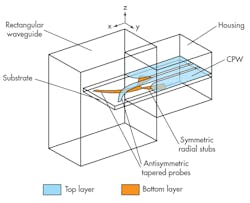
Figure 1 shows the configuration for the proposed transition between rectangular waveguide and CPW. The transition consists of rectangular waveguide, antisymmetric tapered probes, symmetric radial stubs, and CPW. The rectangular waveguide is standard WR-28 with dimensions of 7.112 × 3.556 mm, which will ensure single-mode TE10 propagation at Ka-band frequencies.
RT/Duroid 5880 PCB material was used as the circuit substrate material for the transition; the PCB material has relative permittivity of 2.22, loss tangent of 0.009, and thickness of 0.254 mm. The waveguide-to-CPW transition is a planar, double-sided circuit. CPW is fabricated on the top of the substrate, symmetric radial stubs are fabricated on the bottom of the substrate, and antisymmetric tapered probes are fabricated on both sides of the substrate.
This file type includes high resolution graphics and schematics when applicable.
A Closer Look
This file type includes high resolution graphics and schematics when applicable.
The antisymmetric tapered probe was introduced in the design of a waveguide-to-microstrip transition.17 In this earlier design, the microstrip is a double-layer transmission line while the CPW is a uniplanar transmission line, where the signal line and the two ground planes are on the same side of the substrate. As shown in Fig. 1, the antisymmetric tapered probe is inserted into the center of a standard waveguide E-plane. The CPW is within a metal housing with dimensions of 3.556 × 3.556 mm, which ensures only CPW-mode propagation at Ka-band frequencies.
The center strip of the CPW is directly connected to the top probe of the antisymmetric probes. The bottom probe of the antisymmetric probes is connected to symmetric radial stubs, which provide vertical coupling for changing the direction of the electric field. For the CPW, the magnitude of the current on each ground plane is one-half that of the center strip. Due to this CPW characteristic, it requires two symmetric radial stubs connected to the ends of the bottom of the antisymmetric probes.
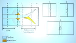
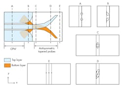
Figure 2 shows the cross-sectional E-field distribution for the proposed transition. The E-field is parallel to the X/Y plane in the CPW section. The radial stubs serve to change the direction of the E-field from parallel to vertical. The antisymmetric tapered probes then transform the z-polarized E-fields energy in the input port of the antisymmetric tapered probes to the y-polarized E-field energy of the TE10 mode in the rectangular waveguide. In this way, the CPW E-field can smoothly change to the TE10 E-field mode in rectangular waveguide.
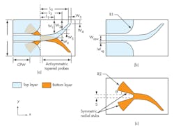
Figure 3(a) shows the schematic circuit for the proposed transition, while Fig. 3(b) presents the circuit layout on the top side of the substrate. The characteristic impedance of the CPW was set to 75 Ω, with the widths of the input ports of the antisymmetric probes chosen accordingly. Ground planes are circularly tapered to minimize reflections, with radius R1 set to 1 mm. The two antisymmetric probes are also tapered in a smooth outline to obtain a good reflection coefficient.
Figure 3(c) depicts the circuit layout on bottom sides of the substrate. The end of the bottom probe is directly connected to the two symmetric radial stubs. The radial stubs are rotated with an optimal angle of 16 deg. to smoothly change the electric field from a y-axis direction to a z-axis direction. The overlap area between the radial stubs and the CPW ground planes should be optimized to provide sufficient electromagnetic (EM) coupling and to minimize reflections.
The radial stub is optimized with a radius, R2, of 1.85 mm and an angle of 31 deg. The length of the entire transition circuit is approximately 4.6 mm. No air bridge is needed for this transition due to the symmetric structure of the radial stubs. Figure 4 shows the fabricated substrate of the transition circuit.
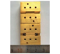
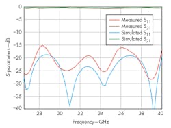
The proposed transition was simulated and optimized using the High-Frequency Structure Simulator (HFSS) EM simulation software from Ansoft Corp. The dimensions of the transition circuit are shown in Fig. 3. The final value of the parameters are Wcpw = 0.55 mm, Wsg = 0.15 mm, W1 = 1.4 mm, W2 = 1 mm, W3 = 0.26 mm, W4 = 0.4 mm, W5 = 0.38 mm, W6 = 0.5 mm, L1 = 1.38 mm, L2 = 2.13 mm, and L3 = 2.74 mm. To experimentally evaluate the performance of the proposed transition, two identical transitions were cascaded back to back.Figure 5 shows the fabricated back-to-back transitions. Measurements were made with a commercial vector network analyzer (VNA) and a pair of coaxial-line-to-waveguide adapters. A thru-reflect-line (TRL) calibration was performed at the WR28 access points. Figure 6 shows the simulated and measured results of the back-to-back transitions, which are in close agreement. The measured results show that the insertion loss of back-to-back transition is less than 0.7 dB, with better than 15-dB return loss from 26.5 to 40 GHz. This implies that the insertion loss of a single transition is less than 0.35 dB across Ka-band frequencies.
In short, a broadband waveguide-to-CPW transition has been proposed based on tapered probes and symmetric radial stubs. Neither an air bridge nor an intermediate transition is needed for this transition, making it relatively easy to fabricate. To demonstrate the effectiveness of the design approach, a Ka-band back-to-back transition was fabricated and measured, with close agreement between simulated and measured results Given its advantages of ease of fabrication, compact size, and low loss, such a broadband transition should be attractive for a wide range of millimeter-wave applications.
Acknowledgment
This work was supported by the Fundamental Research Funds for the Central Universities of China under Grant No. ZYGX2012J030.
Jun Dong, Doctoral Candidate
Ziqiang Yang, Associate Professor
Yu Liu, Associate Professor
Tao Yang, Professor
School of Electronic Engineering, University of Electronic Science and Technology of China, No.2006, Xiyuan Ave, West Hi-Tech Zone, Chengdu 611731, People’s Republic of China
This file type includes high resolution graphics and schematics when applicable.
References
This file type includes high resolution graphics and schematics when applicable.
1. J. Gao, L. Zhu, W. Menzel, and F. Bögelsack, “Short-circuited CPW multiple-mode resonator for ultrawideband (UWB) bandpass filter,” IEEE Microwave & Wireless Components Letters, Vol 16, March 2006, pp. 104-106.
2. X.R. Zhang, Q.Y. Wang, and J.H. Cao, “UWB Waveguide Bandpass Filter With A Narrow Notched Band,” Journal of Electromagnetic Waves and Applications, Vol. 26, 2012, pp. 1116-1124.
3. G.E. Ponchak and R.N. Simons, “A new rectangular waveguide to coplanar waveguide transition,” in Proceedings of the IEEE MTT-S International Microwave Symposium Digest, May 1990, pp. 491-492.
4. G.C. Dalman, “New waveguide to coplanar waveguide transition for centimetre and millimetre wave applications,” Electronic Letters, Vol. 26, 1990, pp. 830-831.
5. M. Khallouk, B. Svensson, and P. Ligander, “CPW-to-waveguide transition using three-step Chebyshev transformer,” Electronic Letters, Vol. 40, November 2004, pp. 1541-1542.
6. V.S. Möttönen and A.V. Räisänen, “Novel wide-band coplanar waveguide-to-rectangular waveguide transition,” IEEE Transactions on Microwave Theory & Techniques, Vol. 52, August 2004, pp. 1836-1842.
7. V.S. Möttönen, “Wideband coplanar waveguide-to-rectangular waveguide transition using fin-line taper,” IEEE Microwave Guided Wave Letters, Vol. 15, 2005, pp. 119-121.
8. S. Kumawat, M.B. Mahajan, and R. Jyot, “Development of Coplanar Waveguide to Rectangular Waveguide Transition,” 2009 Annual IEEE India Conference (INDICON), Vol. 4, December 2009, pp. 18–20.
9. D.-H. Ko, J.-Y. G Moon, D. An, M.-K. Lee, S.-J. Lee, J.-M. Jin, Y.-S. Chae, S.-W. Yun, S.-D. Kim, H.-M. Park, and J.-K. Rhee, “V-band waveguide-to-coplanar waveguide transition for 60 GHz wireless LAN application,” 34th European Microwave Conference, Vol. 2, October 2004, pp. 641-644, 12-14.
10. A. Ramdane, E. Richalot, O. Picon, J. Puech, and L. Lapierre, “Rectangular waveguide-to-CPW transition without air-bridge in the Ka-band,” Microwave & Optical Technology Letters, Vol. 49, January 2007, pp. 510-513.
11. T.-H. Lin and R.-B. Wu, “CPW to waveguide transition with tapered slotline probe,” IEEE Microwave Guided Wave Letters, Vol. 11, 2001, pp. 314-316.
12. C.-F. Hung, A.-S. Liu, C.-H. Chien, C.-L. Wang, and R.-B. Wu, “Bandwidth enhancement on waveguide transition to conductor backed CPW with high dielectric constant substrate,” IEEE Microwave Guided Wave Letters, Vol. 15, 2005, pp. 128–130.
13. N. Kaneda, Y. Qian, and T. Itoh, “A broadband CPW-to-waveguide transition using quasi-Yagi antenna,” in Proceedings of the IEEE MTT-S International Microwave Symposium Digest, June 2000, pp. 617-620.
14. R.-Y. Fang and C.-L. Wang, “A broadband coplanar waveguide to rectangular waveguide transition using a truncated bow-tie antenna,” in Proceedings of the 38th European Microwave Conference, October 2008, pp. 468-471.
15. R-Y. Fang and C.-L. Wang, “Miniaturized Coplanar Waveguide to Rectangular Waveguide Transition Using Inductance-Compensated Slotline,” IEEE Transactions on Components & Packaging Manufacturing Technology, Vol. 2, October 2012, pp. 1666-1671.
16. R.-Y. Fang, C.-T. Wang, and C.-L. Wang, “Coplanar-to-rectangular waveguide transitions using slot antennas,” IEEE Transactions on Components & Packaging Manufacturing Technology, Vol. 1, May. 2011, pp. 681-688.
17. J.-K. Chuang, R.-Y. Fang, and C.-L. Wang, “Compact and broadband microstrip-to-waveguide transition using antisymmetric tapered probes,” Electronic Letters, Vol. 48, 2012, pp. 332-333.
This file type includes high resolution graphics and schematics when applicable.
