Microstrip Antenna Boosts UWB Gain
This file type includes high resolution graphics and schematics when applicable.
Microstrip antennas offer many benefits, including small size and light weight, along with ease of integration with microwave-integrated-circuit (MIC) and monolithic-microwave-integrated-circuit (MMIC) devices.1 They are well suited for transferring data, voice, and video as part of wireless communications applications,2 but they lack one important property for longer-distance communications: higher gain.3 Fortunately, it is possible to develop a microwave antenna with coplanar-waveguide (CPW) feed that offers radiation patterns with enough gain to serve ultrawideband (UWB) communications applications.
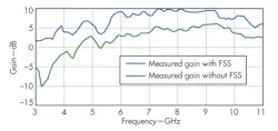
The antenna design features a star-shaped radiation patch with wide impedance bandwidth of 3.0 to 11.7 GHz. Through the use of a three-layer frequency-selective surface (FSS), the antenna can be fabricated with higher gain, enhancing the gain by 4 to 5 dB while maintaining the wide impedance bandwidth. The use of the FSS even helps reduce the antenna’s backlobes.
The bandwidth of a patch antenna is limited if the patch is fabricated on a dielectric substrate that contributes to generation of surface waves, and in so doing reduces the bandwidth of the antenna.3 Numerous techniques are available to increase antenna bandwidth, such as incorporating different slot geometries in the ground planes, or the use of FSS screens, gap-coupled feeds4, and meandered ground planes.5 A UWB antenna with CPW feed can provide the good radiation patterns needed for broad bandwidth.
Antennas for UWB communications can support a wide range of applications, including for microwave imaging, impulse radio communications, and biomedical applications. Increased antenna signal-to-noise ratio is needed for improved gain, and this can be achieved by designing antennas with unidirectional or semi-unidirectional radiation patterns.6,7 The antenna gain can be improved in two ways: by increasing its efficiency or using a reflector surface. For increased efficiency, thinner substrates can be used to provide higher gain due to reduced surface-wave losses.
FSS surfaces are passive periodic structures of metallic or dielectric elements that can be used to control and manipulate the propagation of electromagnetic (EM) waves.8-10 FSS materials can be characterized by means of high surface impedance which retards the propagation of surface waves and supports in-phase reflections of waves striking the FSS surface, resulting in a high gain.11-15 For low-profile antennas, FSS designs should be compact, easy to fabricate, and commercially viable.
By using an FSS screen, it should be possible to improve antenna radiation pattern characteristics, directivity, polarization and, in many cases, bandwidth. FSS materials can be used as a filter, reflector, polarizer, propagation device, or as an artificial magnetic conductor (AMC).16,17 Typical FSS structures already reported in technical literature include square, ring, loop, dipole, and fractal-based shapes. The characteristics and behaviors of these different FSS materials depend on the size, shape, periodicity, and geometric structure of each FSS unit cell.18
To demonstrate the effectiveness of FSS materials and shapes, a wideband FSS form consisting of a rectangular ring element was used to enhance the gain of a star-shaped patch antenna operating from 3.0 to 11.7 GHz. The antenna design was simulated with the help of the CST Microwave Studio computer-aided-engineering (CAE) simulation software from CST, then fabricated and measured using commercial test equipment.
Figure 1 shows the structural details of the antenna. It was printed on one side of 1.58-mm-thick FR-4 circuit laminate with relative permittivity (εr) of 4.3 in the z-axis of the material and loss tangent (tan δ), or dissipation factor of 0.019 in the z-axis of the material. Initially, a simple symmetric rectangular-shaped slot was etched on the ground plane. A double-stepped CPW feed line with widths of Wlf and Wuf, and terminated on a star-shaped patch, was used to excite the slot. A double-stepped CPW feed was used for better impedance matching. Figure 1 also shows the formation of the star-shaped patch, which was formed by inverting and adding two isosceles triangles having base width Tb and height Th, resulting in the star-shaped structure.
To increase antenna bandwidth, the slot was made asymmetric by adding a rectangular section on one side (Fig. 1). The slot’s asymmetric nature provides an inductive characteristic to counter the capacitive effects of the patch (produced by the fringing effect). The bandwidth can also be enhanced by changing the size and shape of the slot. The antenna was optimized further for miniaturization, with optimized parameters shown in the table.
The return loss of the fabricated antenna was measured using a model R&S ZVA-40 vector network analyzer (VNA) from Rohde & Schwarz. Figure 2 compares measured and simulated return loss for the antenna. The measured impedance bandwidth of the antenna is 8.7 GHz (3.0 to 11.7 GHz). From Fig. 2, it can be seen that measured and simulated results are in close agreement except at certain frequencies, where deviations may be due to substrate impurities or deviations because of SMA connectors.
This file type includes high resolution graphics and schematics when applicable.
Assessing Assymmetry
This file type includes high resolution graphics and schematics when applicable.
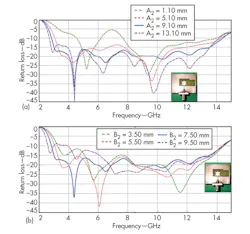
To study the effect of asymmetric slot on the return loss of the antenna, the two slot dimensions, A2 and B2, were varied. Figure 3 shows how return loss changes with variations in these slot dimensions. From Fig. 3(a), it can be seen that as the value of A2 increases, the return loss improves and frequency shifts downward. As A2 increases, the overall slot length increases, resulting in a shift towards lower frequencies. Also, the coupling between the ground and the radiating patch improves with increasing value of A2. This results in better impedance matching and improvement in return loss.
However, after a particular value of A2, the return loss deteriorates with increasing value of A2. So the value of A2 must be optimized; the optimum value was found to be 9.10 mm. From Fig. 3(b), it can be seen that B2 has a similar effect on return loss as A2. The optimized value of B2 was found to be 7.50 mm.
As opposed to the asymmetrical slot shown in Fig. 1, if the slot is extended on both sides, it again becomes symmetrical. The effects of this extended symmetric slot on antenna return loss were studied, and found not ideally suited for UWB operation, even when the slot dimensions are optimized. These return-loss characteristics were studies by considering surface-current distribution for the antenna. High current distribution was found at 4.3 GHz, due to the star-shaped patch, with a resonance at 6.5 GHz due to second harmonics of 3.2-GHz fundamental signals.
By considering current distribution, the first resonance can be approximated as:
f1 = c/[SL(εeff)0.5] (1)
where:
f1 = the lowest resonance frequency (in Hz);
SL = the slot length (in m and equal to 0.065 m);
c = the speed of light (in m/s); and
εeff is the effective relative permittivity which can be approximated by (εr + 1)/2.
The second resonance frequency can be approximated by considering the height of the patch
to λ/4, and it is given by Eq. 2:
f2 = c/[4L(εeff)0.5] (2)
where:
L = the height of the star-shaped patch.
This file type includes high resolution graphics and schematics when applicable.
Designing The Antenna
This file type includes high resolution graphics and schematics when applicable.
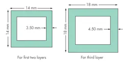
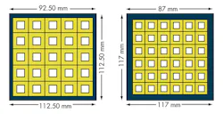
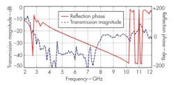
By using loop-type patches, the antenna FSS was successfully designed. Initially, a loop array was printed on one side of the substrate. Then, to increase the stopband bandwidth, different layers of FSS were cascaded to form the final FSS. The FSS is a composite structure with two substrate layers sandwiched between three metallic layers. The 1.6-mm-thick substrate has relative permittivity, εr, of 4.4. The unit element used for all three layers was a loop-type structure, with larger loop for the outermost layer. Figure 4 shows the unit elements used in the different layers of the FSS. The FSS was fabricated with a 6 × 6 element array for two of the layers and 5 × 5 element array for the outermost layer (Fig. 5). Figure 6 shows simulated magnitude of transmission and reflection phase for the FSS. The stopband (transmission less than -20 dB) bandwidth is 8.3 GHz (2.6 to 10.9 GHz). The reflection phase of the FSS is linear which is desirable to increase the gain over a wider bandwidth.
The FSS is mounted below the antenna to enhance the gain, used as a reflector. Waves radiated by the antenna and propagating towards the FSS are reflected by the FSS. If the waves radiated by the antenna and reflected by the FSS are in phase, antenna gain will be increased. The condition for the reflected waves from the FSS and the radiated waves from the antenna to be in phase is given by
ΦFSS -2βh = 2nπ
where:
n = …-2, -1, 0, 1, 2,… (3)
and
ΦFSS = the reflection phase of the FSS;
β = the propagation constant in free space; and
h = the height between the FSS and the antenna.
By using Eq. 1, h can be calculated as 26.13 mm.
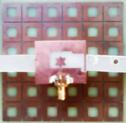
shows the fabricated antenna prototype along with the FSS. The measured impedance bandwidths with and without the FSS are nearly same and equal to 8.7 GHz (from 3.0 to 11.7 GHz). The slight difference between the reflection coefficients (with and without FSS) is due to multiple reflections caused by the FSS.
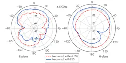
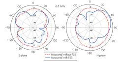
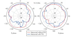
The radiation patterns of the proposed antenna with and without the FSS were measured in an in-house anechoic chamber, with a double-ridged horn antenna used as the reference antenna. Figure 8 compares measured radiation patterns of the antenna with and without the FSS. The radiation patterns without the FSS show a bidirectional nature in the E-plane and omnidirectional nature in the H-plane.
The radiation pattern becomes more directional with application of the FSS. The backlobes are reduced by around 10 dB (at 7.5 GHz) with the FSS. Figure 9 shows the measured peak gain comparison of the antenna without and with the FSS. It reveals an improvement in the peak gain of around 4 to 5 dBi throughout the band after application of the FSS.
In summary, a compact slot antenna with FSS provides high gain for UWB applications. The slot is asymmetrically placed in the ground plane to improve impedance matching. The antenna design offers a measured impedance bandwidth of 102% at a center frequency of 7.5 GHz. To boost gain, a three-metal-layer FSS is used as a reflector, providing improvement of 4 to 5 dBi in peak gain.
Raj Kumar, Senior Engineer
Tuhina Oli, Engineer
Nagendra, Engineer
R.V.S. Ram Krishna, Engineer
Armament Research and Development Establishment (ARDE), Pashan, Pune-411 021, India
Defense Institute of Advanced Technology (DIAT), Deemed University, Girinagar, Pune-411 025, India
This file type includes high resolution graphics and schematics when applicable.
References
This file type includes high resolution graphics and schematics when applicable.
1. C.A. Balanis, Antenna Theory Analysis and Design, Wiley-Interscience, New York, 2005.
2. G.Z. Rafi and L. Shafai, “Wideband V-Slotted Diamond- Shaped Microstrip Patch Antenna,” Electronic Letters, Vol. 40, No. 19, 2004, pp. 1166-1167.
3. Hsing-Yi Chen and Yu Tao, “Antenna Gain and Bandwidth Enhancement Using Frequency Selective Surface With Double Rectangular Ring Elements,” 9th International Symposium on Antennas Propagation and EM Theory (ISAPE) Guangzhou, PRC, November 29-December 2, 2010, pp. 271-273.
4. P.S. Hall, “Probe Compensation in Thick Microstrip Patches,” Electronic Letter, Vol. 23, No. 11, 1987, pp. 606-607.
5. J.S. Kuo and K.L. Wong, “A Compact Microstrip Antenna with Meandering Slot in the Ground Plane,” Microwave and Optical Technology Letters, Vol. 29, No. 2, April 2011, pp. 95-97.
6. A. Pirhadi, H. Bahrami, and J. Nasri, “Wideband high directive aperture coupled microstrip antenna design by using a FSS superstrate layer,” IEEE Transactions on Antennas and Propagation, Vol. 60, No. 4, April 2012, pp., 2101-2106.
7. N. Kushwaha and R.Kumar, “Design of slotted ground hexagonal microstrip patch antenna and gain improvement with FSS screen,” Progress In Electromagnetics Research B, Vol. 51, 2013, pp. 177-199.
8. R. Ulrich, “Far-infrared properties of metallic mesh and its complementary structure,” Infrared Physics, Vol. 7, No. 1, 1967, pp. 37-50.
9. T.K. Wu, Frequency Selective Surface and Grid Array, Wiley, New York, 1995.
10. M.A. Hiranandani, A.B. Yakovlev, and A.A. Kishk, “Artificial magnetic conductors realized by frequency-selective surfaces on a grounded dielectric slab for antenna applications,” IEE Pro.-Microwave Antennas Propagation, Vol. 153, No. 5, October 2006, pp. 487-493.
11. Liang and H.Y. David Yang, “Radiation characteristics of a microstrip patch over an electromagnetic bandgap surface,” IEEE Transactions on Antennas & Propagation, Vol. 55, No. 6, June 2007, pp. 1691-1697.
12. D. Sievenpiper, L. Zhang, R.F. Jimenez Broas, N.G. Alex’opolous, and E. Yablonovitch, “High-impedance electromagnetic surfaces with a forbidden frequency band,” IEEE Transactions on Microwave Theory & Techniques, Vol. 47, No. 11, November 1999, pp. 2059-2074.
13. X.L. Bao, G. Ruvio, M.J. Ammann, and M. John, “A novel GPS patch antenna on a fractal hi-impedance surface substrate,” IEEE Antennas & Wireless Propagation Letters, Vol. 5, 2006, pp. 323-326.
14. B.A. Munk, Frequency Selective Surfaces - Theory and Design, Wiley, New York, 2000.
15. R. Dickie, R. Cahill, H. Gamble, V. Fusco, M. Henry, M. Oldfield, P. Huggard, P. Howard, N. Grant, Y. Munro, and P. de Maagt, “Submillimeter wave frequency selective surface with polarization independent spectral responses,” IEEE Transactions on Antennas & Propagation, Vol. 57, No. 7, July 2009, pp. 1985-1994.
16. C.N. Chiu, C.H. Kuo, and M.S. Lin, “Bandpass shielding enclosure design using multipole-slot arrays for modem portable digital devices,” IEEE Transactions on Electromagnetic Compatibility, Vol. 50, No. 4, November 2008, pp. 895-904.
17. B.A. Munk, P. Munk, and J. Pryor, “On designing Jaumann and circuit analog absorbers (CA absorbers) for oblique angle of incidence,” IEEE Transactions on Antennas & Propagation, Vol. 55, No. 1, January 2007, pp. 186-193.
18. M. Xu, T.H. Hubing, I. Chen, T.P. Van Doren, I.L. Drewniak, and R.E. DuBroff, “Power-bus decoupling with embedded capacitance in printed circuit board design,” IEEE Transactions on Electromagnetic Compatibility, Vol. 45, No. 1, February 2003, pp. 22-30.
This file type includes high resolution graphics and schematics when applicable.
About the Author

Leaders relevant to this article:


