Multilayer Organic Capacitors Exhibit Exceptionally Low Dielectric Absorption
This file type includes high resolution graphics and schematics when applicable.
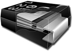
Dielectric absorption (DA) is a condition where residual charge remains stored in a capacitor even after it has been discharged. This could lead to voltage errors in sensitive circuits, such as sample/hold (S/H) circuits, which depend upon the voltage of the capacitor remaining static between measurements. A four-page application note from AVX, “Dielectric Absorption Of Multilayer Organic (MLO™) Capacitors,” discusses dielectric absorption of various dielectric materials while highlighting the MLO capacitors’ low dielectric absorption.
Dielectric absorption is measured as a percentage of the recovered voltage after discharge over the maximum of the original voltage applied. Dielectric materials with lower permittivity constants (k) tend to exhibit lower DA than higher k dielectric materials. DA can range from 0.001% to 10%. Different dielectric materials also have different DA properties. This leads to additional design consideration for S/H circuits, as the recovered voltage could lead to error on the voltage output of the circuit.
The test performed on an MLO capacitor was based on measurement standard MIL-C 19778 using a 2-x-2-in. laminate core for the device. After charging the MLO capacitor for 1 hour at +250 VDC, the device was discharged with a 50-Ω resistor. The voltage across the device was measured 15 minutes after complete discharge. Comparing several dielectric materials, including multilayer glass and ceramic disc dielectric materials with a DA of 0.05%, the MLO capacitor measured a much lower DA of 0.0015%. (Additional information on the test performed, along with a circuit diagram, is available here.)
Other benefits of MLO technology include low-loss performance over wide frequency ranges, repeatable fabrication via a non-fired fabrication process, construction as thin as 0.45 mm, and the capability to create heat pipes with viaholes. It also boasts matched coefficient of expansion to FR-4 circuit boards, multiple RF dielectric layers (which allow for shielded internal electrodes/traces), routing/bonding pads for surface-mount-technology (SMT) components, and moisture uptake typically under 0.04%. These benefits could be considered advantages over traditional ceramic and low-temperature co-fired-ceramic (LTCC) processes.
AVX Corp., 1 AVX Blvd., Fountain Inn, SC 29644; (864) 967-2150.
This file type includes high resolution graphics and schematics when applicable.
About the Author

Nancy Friedrich
RF Product Marketing Manager for Aerospace Defense, Keysight Technologies
Nancy Friedrich is RF Product Marketing Manager for Aerospace Defense at Keysight Technologies. Nancy Friedrich started a career in engineering media about two decades ago with a stint editing copy and writing news for Electronic Design. A few years later, she began writing full time as technology editor at Wireless Systems Design. In 2005, Nancy was named editor-in-chief of Microwaves & RF, a position she held (along with other positions as group content head) until 2018. Nancy then moved to a position at UBM, where she was editor-in-chief of Design News and content director for tradeshows including DesignCon, ESC, and the Smart Manufacturing shows.

