Filters employing substrate-integrated-waveguide (SIW) technology can achieve high selectivity with low passband insertion loss. By way of demonstration, a narrowband, second-order, dual-mode SIW filter was designed for use at 11.3 GHz. Following computer software simulations, the filter was fabricated and found to have high rejection and low passband insertion loss around the center frequency. The filter includes a square SIW cavity, two coupling metalized vias (CMVs), and input/output microstrip lines. Two CMVs in the corner of the cavity provide coupling between degenerate modes.
Pseudo-elliptic filters with finite transmission zeros are not new, but have been widely studied in the literature.1-3 The main challenge in developing these pseudo-elliptic filters is to achieve an asymmetric response.2,3 Dual-mode filters that support cross-coupled network can be designed to satisfy the asymmetric response.
Filters based on SIW technology are useful in microwave integrated circuits (MICs), for a wide range of applications in communications, for suppressing unwanted responses and interference. Learning to implement SIW technology on MIC printed-circuit boards can be instructive, as well as add a great deal of value to both active and passive microwave circuits.
For example, SIW technology has been widely used for a number of different types of microwave filters.4-9 To demonstrate the use of the technology, a narrowband dual-mode second-order filter based on SIW technology with an asymmetric response was designed and fabricated. The filter employs two CMVs for coupling between degenerate modes. The filter achieves two right-handed transmission zeros as a result of source-load coupling and the CMV position.
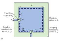
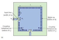
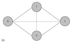
1. The physical configuration of the SIW filter (a) is shown next to (b) the basic filter topology.
The configuration of the proposed dual-mode SIW filter is shown in Fig. 1(a). The filter is constructed by a square SIW cavity, input and output microstrip lines, and two CMVs. The two CMVs perturb the electromagnetic (EM) fields and produce an orthogonal mode.
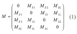
To design a dual-mode filter, a lowpass prototype of the cross-coupled network is first developed, based on the filter topology. In the case of the current filter design, the configuration is a second-order, cross-coupled filter with source load topology as shown in Fig. 1(b). This type of filter topology is capable of providing an asymmetric pseudo-elliptic response. Circuit synthesis can be used to derive the values of the coupling coefficients between the resonators. Synthesis of such cross-coupled filters with an asymmetric response has been determined previously, as noted in the literature.3 Using filter synthesis and considering the filter topology, the generalized coupling matrices that are obtained are shown by Eq. 1:
Denormalization of the coupling coefficients can be performed through the application of the following formulas3:
where:
kij = the normalized coupling coefficient;
Qe = the external quality factor;
fr = the center frequency of the filter; and
BW = the absolute bandwidth of the filter.
The input and output coupling values, Ms1 and MI2, are produced by the input and output microstrip lines. The two CMVs provide the degenerate-mode coupling, MI2. These coupling viaholes have different radii with a 90-deg. angle difference to produce the desired coupling values for an asymmetric response. The radii of the CMVs—namely, r1 and r2, and their distance from the waveguide wall, h—determine the coupling values. Moreover, the dimensions of the square SIW cavity are obtained based on the transverse electromagnetic (TE) modes, TE201 and TE102, as follows:
where:
er = the permittivity;
Le = the effective length of the square SIW cavity; and
c0 = the speed of light in a vacuum.
The value of Le can be obtained from Eq. 45:
where:
d = diameter of the metalized viaholes;
L = the length of the square cavity; and
S = the center-to-center distance between the two adjacent metalized viaholes, as shown in Fig. 1(a).
To demonstrate the effectiveness of this design approach, the proposed dual-model SIW filter was designed using the coupling matrices. It was fabricated on RT/duroid® 5880 circuit material from Rogers Corp. with relative permittivity of 2.2 and substrate width of 0.508 mm. The overall dimensions of the filter, with layout shown in Fig. 1(a), are: L = 20 mm, h = 2 mm, r1 = 0.3 mm, r2 = 0.4 mm, S = 1.3 mm, d = 0.4 mm, W0 = 1.55 mm, Wi = 0.15 mm, and Wt = 1.255 mm.
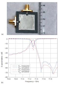
2. The photograph (a) shows the SIW filter fabricated on commercial circuit-board material, while the S-parameters show measured and simulated S11 and S21 responses.
Figure 2(a) shows the simulated and measured scattering (S) parameters for the proposed filter, with a photograph of the fabricated filter in Fig. 2(b). As can be seen, two transmission zeros are created on the right-hand side of the filter response and the selectivity of the filter has been improved. The fabricated filter has return loss of 15 dB and insertion loss of only 1.8 dB across the filter’s 40-MHz passband bandwidth, which is centered at 11.3 GHz.
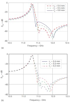
3. The simulated S21 responses were generated for different values of CMV radius.
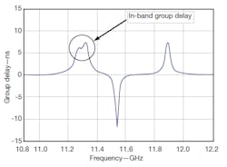
Displacement of the transmission zeros is possible by changing the CMV radii. Figure 3 shows a parametric study of the position of the transmission zeros for different values of CMV radii. Figure 3(a) shows the effects of having the radius of the smaller CMV at a fixed value and the radius of the larger CMV varied. When the difference between the two CMV radii increases, the spacing between the two transmission zeros increases. Figure 4 shows the group delay for the proposed SIW filter. As is apparent from the response curve, the in-band group-delay variation is less than 4 ns for the SIW filter.
4. The group delay shows very little variation within the SIW filter’s passband.
In summary, the proposed second-order, dual-mode SIW filter uses two right-hand transmission zeros to achieve high selectivity. By adjusting the radii of the two CMVs, it is possible to change the position of the two transmission zeros in the filter’s out-of-band response. Comparisons of simulated and measured responses for this experimental filter agree closely, showing that the design is well behaved and predictable.
Ali Frontanpour, Research Engineer
Satellite Communications Group (SCG), Iran Telecommunication Research Center (ITRC), Tehran, Iran; e-mail: [email protected].ALI FOUDAZI,Research Engineer, Satellite Communications Group (SCG), Iran Telecommunication Research Center (ITRC), Tehran, Iran; e-mail: [email protected].
Leila Mohammadi, Faculty Member
Satellite Communications Group (SCG), Iran Telecommunication Research Center (ITRC), Tehran, Iran; e-mail: [email protected].
References
1. A.E. Atia and A.E. Williams, “Narrow bandpass waveguide filters,” IEEE Transactions on Microwave Theory & Techniques, Vol. 20 (1972), pp. 258-265.
2. R.J. Cameron and J.D. Rhodes, “Asymmetric realizations for dual-mode bandpass filters,” IEEE Transactions on Microwave Theory & Techniques, Vol. MTT-29 (1981), pp. 51-58.
3. P. Jarry and J. Beneat, Advanced design techniques and realization of microwave and RF filters, Wiley, Hoboken, NJ, 2008.
4. B. Potelon, J.F. Favennec, C. Quendo, E. Rius, C. Person, and J. C. Bohorquez, “Design of a substrate integrated waveguide (SIW) Filter using a novel topology of coupling,” IEEE Microwave and Wireless Component Letters, Vol. 18 (2008), pp. 596-598.
5. X.P. Chen and K. Wu, “Substrate integrated waveguide cross-coupled filter with negative coupling structure,” IEEE Transactions on Microwave Theory & Techniques, Vol. 56 (2008), pp. 142-149.
6. Y. Dong and T. Itoh, “Substrate integrated waveguide negative order resonances and their applications,” IET Microwave Antennas & Propagation, Vol. 4 (2010), pp. 1081-1091.
7. W. Shen, X.W. Sun, W.Y. Yin, J.F. Mao, and Q.F. Wei, “A novel single-cavity dual mode substrate integrated waveguide filter with non-resonating node,” IEEE Microwave and Wireless Component Letters, Vol. 19 (2009), pp. 368-370.
8. Y. Dong, Y. Wang, and Wei Hong, “A novel substrate integrated waveguide equivalent inductive-post filter,” International Journal of RF and Microwave Computer-Aided Engineering, Vol. 18 (2008), pp. 141-145.
9. R.Q. Li, X.H. Tang, and F. Xiao, “Substrate integrated waveguide dual-mode filter using slot lines perturbation,” Electronic Letters, Vol. 46 (2010), pp. 845-846.
