Keep Abreast of RF Filtering Trends (Part 2)
Download this article in PDF format.
What you’ll learn:
- Higher operating frequencies are driving a shift away from lumped-element designs to distributed-element approaches.
- Differing approaches to conducting an electromagnetic wave through a transmission line or waveguide.
- A comparison of the characteristics of waveguides and transmission lines.
In the opener of our two-part RF filtering trends series, we discussed several emerging trends affecting the “jobs” RF filters need to perform. The article provides details on the overarching trend for mainstream applications to operate at increasingly high frequencies, resulting in the adoption of new RF architectures and new jobs for filters, as well as several trends surrounding RF-filter performance considerations.
In part two, we take these ideas further by focusing on trends in today’s filtering technology options and discussing filtering solutions that can help RF filter designers stay on top of those trends.
Higher Frequencies Drive a Shift
As operating frequencies increase for many applications—which means the shrinking in size of many RF devices—there’s an industry-wide trend to move away from using traditional lumped-element designs. In general, the lumped-element model doesn’t work well at higher frequencies because it’s difficult to manufacture the necessary discrete values without causing several other issues. Let’s look at an example of a bandpass filter tee circuit centered at 28 GHz (Fig. 1).

In this circuit, the series capacitance values need to be low, around 0.0094 pF, and shunt L values need to be around 0.027 nH, which are challenging to achieve with a lumped-element model. First, when using a wire-bond inductor, the coupling between each wire wrap will introduce a small amount of capacitance. The effect of this parasitic capacitance is magnified at higher frequencies, leading to self-resonance.
In addition, board-level parasitic effects result from mounting components and the transmission lines used in a lumped-element model. At high frequencies, these effects would essentially detune a filter. Thus, the small values needed in the example in Figure 1 are difficult to produce because of the physical limits of manufacturing and tolerances noted here.
Therefore, at higher frequencies, RF engineers are shifting to a distributed-element model. As a result, transmission lines and waveguides are the primary methods for transferring electromagnetic waves around a circuit. Simply put, a transmission line is a two-conductor structure, and a waveguide is a single conductor with a hollow metal tube that provides distributed inductance with the empty space between providing distributed capacitance.
Furthermore, RF engineers can use different physical structures to move electromagnetic waves through a transmission line or waveguide. We can define the differences between the structures by looking at the modes each supports. In short, each mode describes a solution to Maxwell’s equations with the boundary conditions for a given structure. That gives us the following three modes:
Transverse magnetic (TM) mode
The electric (E) field has components in the z-direction along the direction of propagation and the magnetic (H) field is transverse at right angles to the z-direction. Therefore, there’s only an electric field along the direction of propagation (Fig. 2).

Transverse electric (TE) mode
This has E-field components at right angles to the z-direction, meaning there’s only a magnetic field along the direction of propagation (Fig. 3).
Transverse electromagnetic (TEM) mode
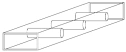
This has both E- and H-field components at right angles to the z-direction and no signals in the direction of propagation. Waveguides can’t support TEM mode (Fig. 4).
Comparing Filter Implementations
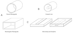
The remainder of this article will look at trends affecting the different types of transmission lines and waveguide filters available today. But first, let’s look at a more general “academic” view of the three main types of transmission lines used today and how the characteristics of these methods compare to the characteristics of a waveguide. The table shows, with all other qualities of the application being equal, how these methods compare, and Figure 5 shows example drawings for each method.

While the table does highlight the traditional limitations of the different implementations, RF engineers are constantly innovating and pushing boundaries to work around some of these traditional constraints. Let’s explore the emerging trends that are helping reduce or eliminate some of the traditional concerns with both waveguides and transmission lines.
Trends Impacting Waveguide-Based Filters
Waveguide filters are, as the name suggests, filters constructed using waveguide technology. In general, the main advantages of a waveguide filter include high Q factor, which occurs as a result of using air as a dielectric, thanks to its high power capacity and near-zero loss. A primary disadvantage of waveguide filters, as illustrated in the table, is the relative size of these structures compared to filters that use a transmission line and can take advantage of TEM modes.
Trend 1: Reducing waveguide filter size with ceramic dielectric resonators To take advantage of some of the other qualities of waveguide filters, such as low loss and high Q, innovative RF filter designers are trying to address the size constraints of waveguide filters by changing the dielectric properties inside the cavity.
For example, one current size-reduction trend is to use ceramic dielectric resonators with a high dielectric constant inside an air-filled waveguide (Fig. 6). Using ceramic instead of air reduces the wavelength of the radiation propagating through the material. This consumes less space, but it comes at a price because there will be higher loss when utilizing a solid dielectric instead of air.
Trend 2: Reducing costs through 3D printing Another overall concern with waveguide filters is fabrication costs, which becomes a big issue when the end device is intended to be a high-volume, low-cost product. Costs are generally high with waveguide filters because precision machining of metal cavities and ceramic components can be expensive and potentially cost-prohibitive in certain applications.
Likewise, one recent trend that may alleviate cost concerns in the future is the use of additive-manufacturing techniques such as 3D printing. Some prototypes have shown it’s possible to employ 3D-printing techniques for components used at frequencies as high as the V band.
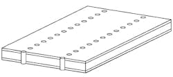
Trend 3: Reducing size and costs with substrate-integrated waveguides One new trend for developing waveguide filters that can address both size and fabrication cost concerns, which Knowles Precision Devices is digging into now, is the use of substrate-integrated waveguides (SIWs). An SIW is basically a rectangular waveguide in which the single conductor walls are formed by plated surfaces and vias, and in which TE mode is used (Fig. 7). That means waves propagate in high dielectric-constant materials.
The key to developing an effective SIW is a thorough understanding of the materials needed to replace the air dielectric as well as the ability to precisely control the structures in a way that isn’t cost-prohibitive. It’s crucial to work with a company that understands the highly engineered materials necessary to provide the right balance between the reduction in size offered by a high dielectric constant versus the potential for loss.
Trends Impacting Transmission-Line-Based Filters
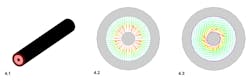
As mentioned, there are three main methods for developing transmission line-based filters: coax, microstrip, and stripline. Let’s first look at transmission-line filter technology using ceramic coaxial TEM-mode resonators (Fig. 4, again). These resonators can be combined with lumped-element components to create filter circuits. As a result, coax transmission lines tend to be used at lower operating frequencies, although this range is usually controlled by the physical dimensions of the resonator and the ceramic material’s dielectric constant.
As noted in the table, the lingering concerns with this approach, which usually involves taking a series of ceramic coax resonators and stringing them together into a circuit, are the size constraints and the difficulty of integrating this type of filter into the wider circuit. However, it’s important to note that relatively small ceramic coaxial resonators can be constructed as a result of continued innovation with material properties. This is still a largely mechanical approach to making filters, though, which may not be ideal because it can require additional “tuning” for the manufacturer.
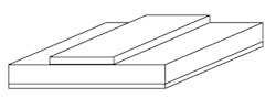
In contrast to the coaxial approach, there’s the relatively easy-to-use microstrip technology for building resonators and the associated circuit elements for filters. At a high level, microstrip is a type of planar transmission line that’s simple to implement in printed circuit boards (PCBs). Composed of a strip conductor, dielectric substrate, and ground plate, microstrip is used in the microwave range with a typical maximum frequency of 110 GHz (Fig. 8).
The main concern with using a microstrip approach, as shown in the table, is the loss experienced compared with other transmission-line and waveguide approaches. However, as noted, the industry is currently innovating on various materials to help address this constraint. The evolution of high-k materials, such as Knowles Precision Devices’ PG, CF, and CG, are helping RF engineers develop low-loss microstrip transmission-line filters.
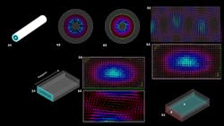
Figure 9 demonstrates how a microstrip transmission-line configuration using Knowles’ PG ceramic reduces loss compared to RO4350 LoPro. Plot A illustrates loss/inch; plot B shows loss/wavelength. Note: We used the same material thickness, metal conductivity, and 50-Ω microstrip transmission line in both configurations.
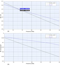
At frequencies above 13.6 GHz, PG material has better overall loss performance. This is largely because the surface roughness of PCBs is about four times greater than that of polished ceramics. Furthermore, as PCB materials are made thinner, the loss delta will become larger due to increasing surface roughness. Therefore, the frequency range in which polished ceramics outperform PCBs will grow. Combined with the benefits of loss/wavelength at higher frequencies, integrating passive RF components on polished ceramics is clearly the lower-loss option compared to PCB materials.
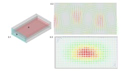
Finally, there’s a stripline approach. Because stripline filters purely use TEM mode, there are clear benefits of stripline over microstrip. First, coupled-line structures don’t need compensation for unequal phase velocities like those that can occur in microstrip. Also, there’s less radiation using stripline. However, the Q, manufacturability, and tolerance all decrease with stripline versus microstrip, which means this method isn’t as good of an option for applications that require higher Q and tighter tolerances.
Follow Trends for Effective Filters
In general, while all RF applications need some level of filtering, there really isn’t a one-size-fits-all RF filtering solution. Additionally, because applications that require RF filters are constantly pushing boundaries, the jobs RF filters can perform must evolve as well to keep up with today’s cutting-edge technologies.
Therefore, it’s imperative for RF engineers to keep pace with the latest trends affecting filter technology, such as those discussed in this two-part series, to ensure they have the most relevant information to develop the best possible filters for their applications. Often, this comes down to knowing the latest trends for materials, especially when it comes to selecting materials that will help address size and cost concerns, and precision manufacturing techniques that can ensure filters maintain high Q and tight tolerances.
About the Author

Peter Matthews
Senior Technical Marketing Manager, Knowles Precision Devices
Peter Matthews is Senior Technical Marketing Manager at Knowles Precision Devices. As a division of Knowles Corporation, Knowles Precision Devices (KPD) focuses on production of a wide variety of highly engineered capacitors and microwave to millimeter-wave components for use in critical applications in military, medical, electric vehicle, and 5G market segments. Peter has over 20 years of experience in technology sales, marketing, and product management.
