This file type includes high resolution graphics and schematics when applicable.
Observation receivers are often employed in radar systems or communications systems to check on the signal quality and activity within a transmit/receive system. When signals are transmitted and received within the same frequency spectrum, observation receivers often employ a common local oscillator (LO) architecture to improve noise performance. The approach is effective for observation receivers for a variety of applications, including communications and radar.
The use of digital predistorton (DPD) in cellular communications base stations, for example, can allow the system’s transmit power amplifier (PA) to operate in its nonlinear region with higher efficiency than is possible in its linear region. The unwanted signal distortion products are reduced or cancelled by intentionally predistorting the transmitted signal waveforms, with the resulting linearized output of the PA being measured by the observation receiver as a means of monitoring signal quality.
Figure 1 (left) shows the use of a common LO for each mixer in the transmit and feedback paths of an observation receiver system. The layout employs a DPD algorithm to correct for the nonlinear distortion of the PA, subtracting and eliminating the unwanted noise and distortion of the LO that mixes with the transmit signal. The common LO approach is also used in radar. However, in a radar system, the primary objective is to improve the dynamic range and target detection capability of the receiver rather than the efficiency of the exciter.
As RF systems evolve—taking advantage of available higher-speed data converters for digitizing and generating signals at RF and microwave frequencies—the common LO approach can be implemented in the digital realm for effective reduction of noise in observation receivers using high-speed, high-resolution analog-to-digital converters (ADCs) and digital-to-analog converters (DACs). System engineers are finding the benefits of using high-speed RF sampling ADCs such as the model ADC32RF45 from Texas Instruments.
Such data converters provide a high level of integration in support of compact observation receivers, at the same time providing a wide frequency range and high sampling speeds that make it possible to eliminate a frequency downconversion stage in a traditional heterodyne receiver design (along with all the associated components).
When using a direct RF sampling data converter in a receiver design, the sampling clock is the equivalent of an LO in an analog receiver with intermediate-frequency (IF) stage (Fig. 1, right). Having a common clock with data converters in RF-sampling-based systems is akin to using a common LO with mixer-based frequency-conversions systems to achieve correlated noise cancellation.
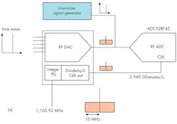
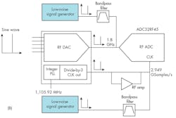
To determine the magnitude of noise cancellation possible by using the common clock approach with multiple data converters in an RF-sampling-based system, a trio of experiments were performed using an RF DAC as the signal source and an RF ADC as the heart of the sampling receiver. In the first experiment, a 10-MHz-wide “noise pedestal” was added as double-sideband noise to the RF DAC’s internal phase-locked loop (PLL) reference clock (Fig. 2a). The RF DAC then produced a 1.8-GHz output signal with the double-sideband noise pedestal. This same RF DAC has the capability to provide a divided clock output, which includes noise pedestals, as the RF ADC’s sampling clock.
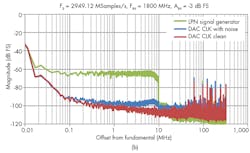
The resulting fast Fourier transform (FFT) plot (Fig. 2b) was normalized to the input signal tone and compared against a spectrally pure input signal from a low-noise signal generator and a sampling clock with noise pedestals, as well as a spectrally pure input signal and clock from the RF DAC with the noise pedestals removed from the reference clock source.
The DAC’s internal PLL has a loop filter bandwidth of about 6 MHz. When using the clean input from the low-noise signal generator (the green trace in Fig. 2b), the rolloff is visible. The FFT comparison reveals some interesting results.
Very close <100-kHz offset) to the carrier, the noise floor appears to be limited by the noise floor of the DAC clock output driver. At offsets from about 100 kHz to about 6 MHz, the noise pedestal receives about 25 to 35 dB attenuation, and the noise floor is close to a setup with noise removed (red trace). As the offset frequency increases, the amount of noise cancellation decreases.
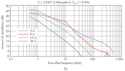
The second experiment explored the effects of phase mismatches between signal and clock inputs on noise cancellation. To realize different phases leading to the two inputs, the length of the cable to the clock input was varied from 3 to 36 in. while the length of the cable to the signal input remained constant at 8 in.
As the test results clearly illustrate, larger phase mismatches between the clock and signal input lines result in more degraded performance. For optimum results, the signal and clock path lengths should be as short and as tightly matched as possible.
Figure 3 provides a comparison of results showing how noise cancellation performance can be improved with shorter clock input cables and longer signal input cables. This suggests that the clock routing on the evaluation and inside the ADC32RF45 is a little longer than the signal path. This is important to remember during the actual printed circuit board (PCB) layout, where isolation between the RF DAC and ADC may be traded off against phase mismatch.
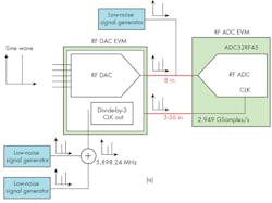
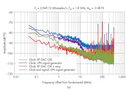
How much noise improvement can be expected in an actual system implementation of the common clock/LO approach? To find out, in the third experiment, a 1.8-GHz sine wave from the RF DAC was sampled using three different options for the ADC’s sampling clock. To provide the recommended clock amplitude for the best ADC noise-floor performance, an RF amplifier was added to boost the clock amplitude (Fig. 4a).
When providing a low-noise sampling clock from the low-noise signal generator, there is no noise cancellation. Hence, the PLL loop filter response is clearly visible in the output spectrum (Fig. 4b, purple curve). Using the clock output from the RF DAC causes the correlated noise to be cancelled. However, insufficient clock amplitude results in a high ADC noise floor that can be observed outside the PLL loop bandwidth (Fig. 4b, blue curve, for offsets greater than 10 MHz).
The best results are achieved when adding the RF amplifier in the clock path to compensate for loss in connections to and from the evaluation modules (EVMs) used to perform these experiments (Fig. 4b, red curve). Better results can be achieved when directly connecting the RF DAC clock output to the ADC clock input on the same circuit board. The far-end noise floor is now limited by the inherent thermal noise of the clock output driver and the ADC32RF45 RF sampling ADC, while the close-in, correlated noise experiences noise cancellation.
The inherent thermal noise of the DAC clock output is worse when compared to the low-noise floor of the low-noise signal generator with a bandpass filter (Fig. 4b, green curve), which occurs with offsets greater than about 50 MHz. However, by taking advantage of noise cancellation, the close-in noise performance (<30 MHz offset) of the RF DAC clock output is actually better (lower), despite its inherently worse internal PLL noise.
The three experiments described above show that the common LO approach for transmitter noise cancellation can also be applied to RF sampling data converters when used in mixed-signal transmitters and receivers. Such RF data converters offer the capabilities to digitize signals in the RF range with wider instantaneous bandwidths than lower-frequency IF data converters, and can also take advantage of the same noise cancellation capabilities as traditional IF-sampling-based data converters.
Tommy Neu, System Engineer
Editor’s Note: The ADC32RF45 is a dual-channel, 14-b analog-to-digital converter (ADC) that features maximum sampling rate of 3.0 GSamples/s. It can effectively digitize input signals to 4 GHz or higher with wide modulation bandwidths, for implementation of low-component-count, direct-conversion receivers. A full review of the new ADC can be found here.
Looking for parts? Go to SourceESB.
This file type includes high resolution graphics and schematics when applicable.


