Clock Jitter Attenuator Cuts BS Noise to 3.2 GHz
This file type includes high resolution graphics and schematics when applicable.
Jitter can be a critical limiting factor in wireless communications systems—for example, curbing clock precision and data converter performance in cellular base stations (BSs). Fortunately, the model HMC7044 3.2-GHz clock jitter attenuator from Analog Devices provides a means of curbing jitter in base stations, thus improving the signal-to-noise (SNR) and dynamic-range performance of their data converters.
The compact packaged integrated circuit (IC) is designed to support the JESD204B serial interface standard for connecting high-speed data converters and field-programmable gate arrays (FPGAs) used in cellular base stations. It features almost negligible 50-fs jitter performance and provides as many as 14 clock outputs for connection to different components.
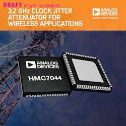
The model HMC7044 jitter attenuator packs a great deal of functionality within a compact 10 × 10 mm, 68-lead LFCSP package (see figure). The package includes two integer-mode phase-locked loops (PLLs), two overlapping-in-frequency, on-chip voltage-controlled oscillators (VCOs), system reference control, serial peripheral interface (SPI) control, and clock distribution circuitry. It is capable of performing reference selection and generation of extremely low-noise signals for data converters with either parallel or serial (such as JESD204B) interfaces.
In fact, the device’s noise floor is -156 dBc/Hz at 2457.6 MHz, while the phase nose is -141.7 dBc/Hz offset 800 kHz from a 983.04-MHz output signal. In the time domain, the root-mean-square (RMS) jitter is no worse than 50 fs and typically 44 ps offset 12 kHz to 20 MHz from 2457.6 MHz. The compact jitter attenuator’s synchronization pin enables a valid interruption of the internal system reference (SYSREF) synchronization control to simplify JESD204B synchronization.
The clock jitter attenuator incorporates enough functionality to design a full cellular BS clock solution with a single device. It provides as many as 14 device clocks for driving a variety of different devices. The HMC7044’s clock outputs can be configured for a number of different signaling standards, including low-voltage differential signaling (LVDS), low-voltage, positive emitter coupled logic (LVPECL), and current-mode logic (CML) clock signals.
The model HMC7044 clock jitter attenuator provides the stable clock signals for synchronization of the various devices within a cellular BS dependent upon clock signals for timing, including data converters and FPGAs. Model HMC7044 includes an input port for use with an external VCO at frequencies to 6 GHz. It operates at a maximum SPI bus frequency of 10 MHz and an input voltage range of -0.1 to +3.6 V dc for digital and bidirectional input signals.
The HMC7044 clock jitter attenuator also offers a wide range of clock management and distribution features that make it possible for designers of base stations to build an entire clock design with a single device. The device is suitable for use in BS microwave baseband cards, for reference frequency distribution for alignment of multiple PLLs in wireless communications systems, and for meeting the clock requirements of multiple data converters in those systems.
In fact, this attenuator represents a practical solution for any application requiring multiple clocks for precise timing. It includes numerous alarms and status indicators to monitor system performance levels, including a loss-of-signal (LOS) indicator to warn of changing signal conditions within a BS or other communications system.
The model HMC7044 jitter attenuator includes on-board voltage regulation for excellent power supply rejection ratio (PSRR). It allows SPI-programmable phase-noise performance versus power consumption to achieve target system performance levels, while also ensuring that the system is operating economically and efficiently. It is a highly integrated device that provides tremendous functionality and performance for a modest investment. P&A: $12.75 (1000 qty.).
Analog Devices, Inc., One Technology Way, P.O. Box 9106, Norwood, MA 02062-9106; (781) 329-4700
This file type includes high resolution graphics and schematics when applicable.
About the Author
Jack Browne
Technical Contributor
Jack Browne, Technical Contributor, has worked in technical publishing for over 30 years. He managed the content and production of three technical journals while at the American Institute of Physics, including Medical Physics and the Journal of Vacuum Science & Technology. He has been a Publisher and Editor for Penton Media, started the firm’s Wireless Symposium & Exhibition trade show in 1993, and currently serves as Technical Contributor for that company's Microwaves & RF magazine. Browne, who holds a BS in Mathematics from City College of New York and BA degrees in English and Philosophy from Fordham University, is a member of the IEEE.


