Clock Source Kills Jitter to 1.25 GHz
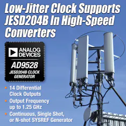
Stable reference clocks are critical for many forms of communications systems, and the AD9528 JESD204B clock and system reference (SYSREF) generator from Analog Devices provides the high-speed/high-frequency performance needed for analog and digital communications systems pushing past data rates of 1.25 GSamples/s. The JESD204B standard is being used increasingly as the interface between digital signal processors (DSPs) and high-speed data converters in gigabit-speed communications systems.
The AD9528 IC contains a two-stage phase-locked loop (PLL) with integrated JED204B SYSREF generator for synchronization of multiple devices. The first PLL stage furnishes input signal reference conditioning by reducing the amount of jitter present on a system clock. The second PLL stage also helps to minimize jitter by providing high-frequency clock signals with low broadband noise. The AD9528 produces two output signals (PLL1 and PLL2) with maximum frequency to 1.25 GHz, and 12 additional low-noise output signals as high as 1 GHz.
Each of the 14 output channels contains a divider that includes coarse digital phase-adjustment capability and analog phase-delay control for manipulation of timing across all 14 output channels. The AD9528 can also be used to serve as a buffer for two high-speed/high-frequency input signals and distribute 14 device clock and/or system reference signals.
By using the on-board timer circuitry, the delay control of the PLL1 output port can be controlled in steps as fine as 17 ps; the delay control of the PLL2 output port can be adjusted in steps as fine as 20 ps. The clock output phase noise depends on the mode of operation and frequency. For example, in single-mode operation, at an output of 122.88 MHz, the single-sideband (SSB) phase noise is -123 dBc/Hz offset 1 kHz from the carrier and -149 dBc/Hz offset 1 MHz from the carrier.
This versatile device aids systems that are using the JESD204B standard for interfaces between data converters and DSPs in a wide range of applications, including for wireless cellular communications systems, defense electronics systems, and RF/microwave test instrumentation systems. It is suitable for clock generation and timing—especially for systems employing multiple mixed-signal ICs, such as analog-to-digital converters (ADCs), digital-to-analog converters (DACs), and direct-signal-synthesizer (DDS) signal sources.
The device is designed for typical supply of +3.3 VDC, 1635 mW typical power consumption in single-loop-mode operation, and 1675 mW typical power consumption in dual-loop-mode operation, with operating temperature range of -40 to +85°C.
Analog Devices, Inc., Three Technology Way, Norwood, MA 02062; (781) 329-4700, (800) 262-5643
About the Author
Jack Browne
Technical Contributor
Jack Browne, Technical Contributor, has worked in technical publishing for over 30 years. He managed the content and production of three technical journals while at the American Institute of Physics, including Medical Physics and the Journal of Vacuum Science & Technology. He has been a Publisher and Editor for Penton Media, started the firm’s Wireless Symposium & Exhibition trade show in 1993, and currently serves as Technical Contributor for that company's Microwaves & RF magazine. Browne, who holds a BS in Mathematics from City College of New York and BA degrees in English and Philosophy from Fordham University, is a member of the IEEE.


