3D Integrated Circuits Show Extreme RF Potential
This file type includes high resolution graphics and schematics when applicable.
Since the 1960s, Moore’s Law has been both a limit and a guide to the rapidly growing integrated-circuit (IC) and semiconductor industries. In recent years, the sophistication of IC and semiconductor fabrication has allowed for new ways to struggle out of the stifling umbrella of Moore’s Law. Strangely enough, the concept of expanding integration to three-dimensional (3D) ICs also was proposed in the same decade as Moore’s famous statement by James Early of Bell Labs.
The industry has shown increasing interest in seeing 3D ICs as a common reality, given the potential power, cost, space, processing time, and interconnect reductions for high-performance applications. There have already been implementations of digital and even analog 3D ICs with the Xilinx Virtex-7 2000T field-programmable gate array (FPGA), which is enabled by stacked-silicon-interconnect (SSI) technology. In addition, AMS AG has invested 25 million Euros in an analog 3D IC process expansion, which can be used with any of its present processes to generate analog 3D ICs using through-silicon-via (TSV) technology.
What does all this mean for the RF and wireless industries? A brief look into ICs’ past may be helpful. The push to meet advancing technical applications with smaller, faster, lower-power, cheaper, and more integrated solutions has been a driving point of the IC and semiconductor industries since the early 1960s. For a while, this evolution was accommodated by decreasing the gate size of transistors by advancing semiconductor processing technology. Without a breakthrough in semiconductor materials or computing technology, scientists at the time realized that there would be a finite limit to the amount of transistors that would fit on a chip. This led to significant advances in material science, computer science, physics, and chemistry.
This was all well and good for the RF community, as RF components at the time were rather large, high-power, discrete components that didn’t have to utilize very high frequencies. The frequency requirements and applications of RF technology changed when the demands on the present frequency bands increased and the urge to send digital data over RF carriers required increasingly faster data rates. This trend led to higher frequency bands, which allowed for RF components to shrink and eventually become integrated.
The demands in the military and commercial wireless industries for more utility and increased integration of handheld and portable devices led to a blending of RF, analog, and digital technologies. This, in turn, led to the development of the first mobile cellular phone in the 1980s by Motorola (Fig. 1). That mobile phone opened the gateway for modern wireless portable-electronic devices (WPEDs) like cell phones, satellite phones, GPS tracking units, and multifunction portable computers/tablets. It also increased the growth of the already fast-growing wireless and RF industries to help meet ever-increasing requirements and demand.
Global sales of consumer WPEDs are expected to reach 73 million units in 2013 and that number is predicted to rise to over 150 million units by 2017, according to the Strategy Analytics report,” Embedded Wireless (WWAN) and LTE CE Devices: Global Market Forecast.” The requirements for expanding the capability of these devices is driving up data rates, range, bandwidth, power requirements, and the need for constant connectivity. Many presently designed WPEDs are already including multiple antennas, which operate in different frequency modes, and the new IEEE 802.11ac and ad standards. Thus, they are only looking to add more burdens to designers of these already cramped and cluttered devices. The solution to these headaches just might be 3D IC technology.
3D ICs could be seen as a huge advancement in enabling technologies. Before now, there were rarely options for high-performance electronics other than separating analog, digital, and RF sets of components. Each of these component blocks requires unique power, heat management, test setup, and interconnects. This usually leads to an increase in cost, space, power, and production time because specialized equipment is required for each block. 3D IC technology could allow for each of the blocks to be incorporated into a single 3D module. Of course, the huge benefits offered by such a technology also has its share of challenges: temperature management, stacking, interlayer connections, parasites, processing time, and yield.
This file type includes high resolution graphics and schematics when applicable.
Competing Approaches
This file type includes high resolution graphics and schematics when applicable.
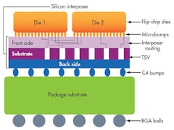
Currently, there are two main technologies that are being implemented and explored for mainstreaming: an advanced die-integration technique using a silicon interposer for an electrical interface, known as 2.5D, and 3D die stacking with TSVs. 2.5D IC integration has the potential to deliver much tighter form factors than standard packaging systems by mounting multiple dies—potentially even dies from different technologies, such as analog, digital, and RF—on a common silicon interposer substrate (Fig. 2). The interconnect wires for the dies are routed through the interposer with the system inputs/outputs (I/Os). Power connections are connected to the underlying package with TSVs, which is an advancement over the flip-chip wire-bonding techniques that are presently used.
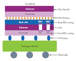
Many consider 3D die stacking to be the technology that offers greater benefit. To create effective 3D stacks, the silicon wafers must be thinned less than 50 μm. The TSVs that interconnect between the layers can then be can be etched into the substrate, like the example in Figure 3. In a heterogeneous system, the bottom die would utilize a silicon interposer much like the 2.5D IC systems. The much smaller footprint, heightened integration, and potentially more streamlined processing of the 3D ICs make them an attractive option. But many production difficulties must be accounted for, such as producing consistent thinned wafers, handling the heat generated by the stack, testing the stack, and managing reasonable yields.
Most of the 3D-IC focus has been on stacking digital blocks to increase data rates, decrease power use, and increase digital density. There are several fabrication facilities and product lines that already utilize early 3D IC technologies to great effect, such as the Xilinx Virtex-7 2000T FPGA.
What Does All This Mean For The Wireless World?
Right now, there is not much in the way of actual products or device solutions, but the future holds a great deal of promise. The benefits for mobile applications—smaller, faster, cheaper, lower power, and more integrated—are right in line with the direction that the industry is taking with WPEDs. The ability to connect several RF die from different technologies with the precision interconnect and small size of IC fabrication processes would be a big win for an industry that has to constantly downsize its footprint. Naturally, this is driving research, modeling, and simulations of 3D IC TSV systems for RF use. With technical papers titled “Characterization of High Performance CNT-based TSV for High Frequency RF Applications” and “Through-Silicon Via Technologies For Interconnects in RF MEMS,” one can imagine that a lot of uses are being found for 3D IC technology. Examples include passive components that span multiple die and even using the TSVs as waveguides, filters, and antennas for millimeter-wave applications.
This file type includes high resolution graphics and schematics when applicable.
About the Author
Jean-Jacques DeLisle
Jean-Jacques graduated from the Rochester Institute of Technology, where he completed his Master of Science in Electrical Engineering. In his studies, Jean-Jacques focused on Control Systems Design, Mixed-Signal IC Design, and RF Design. His research focus was in smart-sensor platform design for RF connector applications for the telecommunications industry. During his research, Jean-Jacques developed a passion for the field of RF/microwaves and expanded his knowledge by doing R&D for the telecommunications industry.


