This file type includes high resolution graphics and schematics when applicable.
Fractional phase-lock-loop (PLL) frequency synthesizers are capable of low phase noise, but spurious noise can be a problem. Such spurious content should not be ignored and is one of the concerns of frequency synthesizer designs and manufacturers.1 Fortunately, using an approach based on variable-reference-frequency technology, it is possible to design and fabricate a fractional PLL synthesizer with better than -75 dBc spurious suppression across the band from 2.6 to 3.2 GHz. This approach uses neither cancellation of quantization noise nor linearization of charge-pump techniques.
Several methods are known for suppressing spurious noise. Use of the analog phase interpolation (API) technique can provide an anti-ramp-up current for the phase frequency detector (PFD) to balance phase errors. Nevertheless, this circuit is complex and must be quite precise to achieve desired performance. API accuracy of at least 0.03% is required for spurious suppression of -70 dBc. The use of a sigma-delta technique can shift spurious signals from close to the carrier to further away from the carrier, using the lowpass character of a PLL, although the spurious content is still considerable at about -60 dBc.2,3 Greater spurious suppression is possible by decreasing the divide ratio of the PLL.
For creating frequency synthesizers with low spurious content, a fractional PLL synthesizer was developed using variable reference frequencies. Most frequency synthesizers are based on PLL and/or direct-digital-synthesis (DDS) methods. In some cases, DDS is used as a reference source for the PLL, or as a fractional divider for a PLL, or to generate signals to mix with the RF feedback path of the PLL.4,5 In the current design, a DDS is used as a fractional divider in the PLL feedback path, clocked from the same PLL output (Fig. 1).
In this design, LPF represents a lowpass loop filter, VCO is a voltage-controlled oscillator, and FREF is the reference frequency. Frequency tuning is achieved by adjusting the output frequency of the DDS with a proper tuning command; a high-frequency prescaler is set to keep the DDS input clock frequency within specified limits. The approach depends on keeping the DDS output equal to the reference frequency for any desired RF output frequency.
Spurious and phase noise within the loop bandwidth are assumed to increase by a factor of 20logN within the PLL bandwidth. The output frequency is N times the reference frequency, and noise outside of the loop bandwidth will be suppressed.6 But if the internal structure of a DDS is included as part of this analysis, the results can be somewhat different. Figure 2 shows a PLL hybrid with a DDS internal structure.
Typically, a DDS will suffer noise from two causes. One is because the phase-addressing sequence of random-access memory (RAM) is longer than the bits of typical digital-to-analog converters (DACs) used in DDS sources. Lower-order digits in the sequence can be abandoned in favor of higher-order digits, resulting in phase truncation errors from the DDS.
The second cause of noise in a DDS is the fact it produces a staircase-type output waveform in which spurious content passes through a nonideal lowpass filter (LPF).7 When a DDS’s reference frequency is correspondingly high and the output frequency is correspondingly low, by properly selecting the output frequency, noise introduced by a nonlinear DAC can be reduced. In this case, for a DDS, close-to-the-carrier spurious content is caused mainly by phase truncation errors.
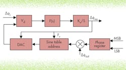
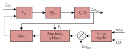
Figure 2 shows the relationship between the phase truncation error, Δφcut, and the output frequency. Since the sinewave table addresses these errors, and an ideal DAC provides a linear response, the components can be regarded as a proportional link which follows the relationships presented in Eq. 1 for open-loop gain, G(s), and in Eq. 2 for the input-output transfer function, H(s):
As clarified by the transfer function, the loop shows that the lowpass characteristic for the phase truncation error, as well as the noise gain in the passband, are not impacted by the frequency-division ratio. The DDS’s phase-noise and spurious characteristics will not be degraded by the loop; thus, the noise in the loop won’t deteriorate by 20logN. The DDS works on the entire loop frequency output like a fractional divider. In fractional frequency programs, fractional spurious products occur, affecting the quality of the output bandwidth and the output signals in typical fractional-N frequency synthesizers.
During each clock period, the DDS completes a phase accumulation cycle. The PFD output voltage, through a lowpass loop, is proportional to any phase difference, which would generate a periodic staircase sawtooth waveform. Equation 3 is the Fourier transform expression of the sawtooth waveform:
where T is the period of the waveform. To maintain N.F times the phase detection frequency, the control voltage is not only present in a DC component, but also in a sinusoidal component of which the frequencies are given by n/T. As a result, modulation spurious products (which degrade the performance of the PLL) occur in the area of N.F(FPFD) ± n(FPFD)(0.F), where FPFD is the frequency of the phase-frequency detector.
For example, for an output frequency that is 16.2 times the reference frequency, this relationship will be 16.2(FPFD) ± n(FPFD)(0.2), where n is 1,2,3,4….
The sinewave component generates a modulated output signal, producing modulation spurious products. As Fig. 3 shows, further optimization of the reference frequency was performed. Results reveal that low-frequency modulation signals in Eq. 3 will completely pass if the frequency offset is less than the loop bandwidth, and modulation spurious signals are correspondingly large. However, when n(FPFD)(0.F) is much larger than the lowpass cutoff frequencies, modulation signals will be suppressed by the lowpass nature of the loop, greatly reducing modulation spurious content.
As a result, the band with large modulation spurious content is in the vicinity of integer multiples of the reference frequency. Assuming a reference frequency 100 MHz with a 50-kHz PLL bandwidth, clean spectrum could be obtained for a 3-GHz output frequency (an integer multiple of 100 MHz). But when the output frequency is in the range of 3 GHz ±500 kHz (except 3 GHz), the output spectrum would contain large modulation spurious content. The modulation spurious content would be gradually suppressed with increasing offset frequency.
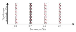
When reaching a certain offset frequency, spurious suppression can reach more than -70 dBc. For modulating spurious content, the farther the frequency offset distance from the carrier and the higher the lowpass loop order is, the stronger the spurious suppression will be. Figure 4 shows the frequency step distribution obtained with these restraints. High resolution is not possible when the frequency falls within the hatched areas, only within the blank area.
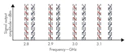
To solve this dilemma, a variable reference frequency was needed and a variable reference source program to determine and change the reference frequency. For example, with reference frequency A, when the output frequency falls within the hatched area, the reference frequency will be changes to a frequency B. The hatched area of frequencies A and B do not overlap. Thus, the hatched area of A becomes the blank area of B, and the original modulation spurious signals will be suppressed by the lowpass loop. By changing the reference frequency, high frequency resolution can be achieved in all these areas (Fig. 5).
This file type includes high resolution graphics and schematics when applicable.
Formulating the Program
This file type includes high resolution graphics and schematics when applicable.
Of course, such a solution depends on finding frequencies A and B. If a frequency C is the result of a common multiple of A and B, then regardless of which frequency is the reference, small frequency steps cannot be reached around C. The least-common multiple of the reference frequency determines the bandwidth of the frequency synthesizer, and the least-common multiple output frequency cannot fall within the required frequency band. To obtain a wider output bandwidth, more prime frequencies are needed to increase the number of least-common multiple, and the frequency of the least-common multiple must apply across the full output frequency range.
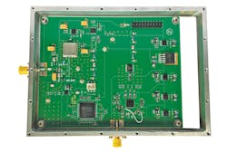
For the current program, 46 and 50 MHz were chosen as reference frequencies to evaluate their differences on synthesizer spurious performance. The reference frequencies were obtained by using the model AD9517-2 PLL chip and model ADG904 switch chip, both from Analog Devices. For the main loop, a model AD9910 from Analog Devices was chosen as the DDS; the model AD4002 from Analog Devices as the PFD; model ROS-3360 from Mini-Circuits as the VCO; model HMC426 from Hittite Microwave Corp. as the prescaler; and model AD8671 from Analog Devices as the loop voltage gain link for the LPF. Figure 6 shows the prototype frequency synthesizer based on these parts.
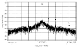
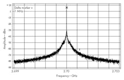
The basic idea of this frequency synthesizer design is to use variable reference frequencies to avoid fractional spurious signals. Figure 7 shows the result of using 50 MHz as the reference frequency and a 100-kHz step to generate a 2.7-GHz output signal, with excessive fractional and intermodulation spurious content. When the frequency step is 100 kHz, fractional spurious content falls within the loop bandwidth, at about -40 dBc.
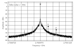
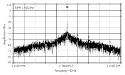
When the step increases to 1 MHz, spurious falls outside of the loop bandwidth, and the fractional spurious suppression is increased to about -60 dBc (Fig. 8). But when the reference frequency is switched to 46 MHz, (not a factor of 2.7 GHz), the performance of Figs. 9 and 10 results, with much less spurious content.
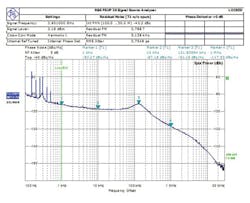
Figure 11 shows the phase noise and spurious content for a 2.9-GHz output with a step size of 1 kHz. The phase noise is -92.19 dBc/Hz offset 1 kHz from the carrier. The spurious suppression is better than -75 dBc for frequency offsets greater than 1 kHz (spurious content for offsets of less than 1 kHz is mainly due to interference from the power supply and the OCXO).
Fang Rui, Master Degree Candidate
Qian Huan-Yu, Engineer
Wu Guo-An, Professor
Institute of Microwave Technology Application, Huazhong University of Science and Technology, Wuhan, 430074, People’s Republic of China
References
1. Haiyong Wang, Guoliang Shou, and Nanjian Wu. An Adaptive Frequency Synthesizer Architecture Reducing Reference Sidebands. IEEE International Symposium on Circuits and Systems, 2006, pp. 3081-3084.
2. Salvatore Levantino, Giovanni Marzin, Carlo Samori, and Andrea L. Lacaita, “A Wideband Fractional-N PLL With Suppressed Charge-Pump Noise and Automatic Loop Filter Calibration,” IEEE Journal of Solid-State Circuits, 2013, pp. 2419-2429.
3. N. Fatahi and H. Nabovati, “Sigma-Delta Modulation Technique for Low Noise Fractional-N Frequency Synthesizer,” 2010 4th International Symposium on Communications, Control, and Signal Processing (ISCCSP), pp. 1-5.
4. Alexander Chenakin, Frequency Synthesizers: Concept to Product, Artech House, Norwood, MA, 2011.
5. A. Bonfanti, F. Amorosa, C. Samori, and A.L. Lacaita, “A DDS-Based PLL for 2.4-GHz Frequency Synthesis,” IEEE Transactions on Analog and Digital Signal Processing, 2003, pp. 1007-1010.
6. Xiao Pu, J. Abraham, A. Thomsen, and K. Nagaraj, “A Novel Fractional-N PLL Based on a Simple Reference Multiplier,” IEEE 54th International Midwest Symposium on Circuits and Systems (MWSCAS), 2011, pp. 1-4.
7. Sadeghi Vahideh Sadat, Saeed Sohail Imran, Shane Calnan, Michael Peter Kennedy, Naimi Hossein Miar, and Mark Vesterbacka, “Simulation and Experimental Investigation of a Nonlinear Mechanism for Spur Generation in a Fractional-N Frequency Synthesizer,” International Signals and Systems Conference (ISSC 2012), IET Irish, 2012, pp. 1-6.
This file type includes high resolution graphics and schematics when applicable.
