In 1944, the United States Army Signal Corps started paying scientists to study materials that could be used in radio equipment. The first substance under investigation was known as barium strontium titanite – a powdered ceramic – which is capable of being altered when shocked with an electric current.
The researchers gave the material a lukewarm review. It could be made into delay lines and filters operating at microwave frequencies, they wrote in a report, but fabricating the material to jump between frequencies posed a significant challenge. Fast forward sixty years and engineers are still struggling with it.
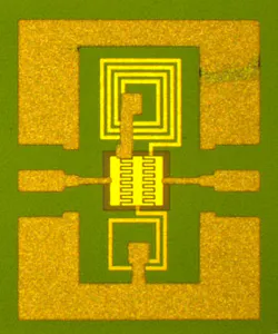
Now, researchers from the University of California, Santa Barbara, recently announced a new method for shaping the barium compound into circuits – ones that can be reconfigured to access multiple frequencies. By reducing the amount of heat radiated from the material, the researchers were able to create smaller and more efficient circuits.
The work, which was based out of the UCSB Materials Research Lab, and which appeared in the journal Applied Physics Letters, breathes life into a material considered defective by chip industry standards. The material is only used in a small number of wireless capacitors, which are paired with antennas to tune into different frequencies.
But the barium compound has potential. It could be used “to create tunable antennas for cellular communications, which allows a small antenna to be tuned over a wide frequency range or enables a phone to adapt to different surroundings for improved efficiency and battery life,” said Robert York, an electrical engineering professor, in an article published with the research.
He also suggested the material could be used to create phase-shifters for phased-array antennas in satellite communications.
Materials like barium strontium titanate are known for having high dielectric constants, meaning that they can be adjusted with a pulse of high voltage electricity. The National Institute of Standards and Technology, which sponsored the research in 1944, is studying dielectrics to enable satellites and smartphones to tune into precise frequencies. Many chipmakers like Intel and Samsung are eyeing the materials to shrink computer circuits toward the atomic level.
These qualities have been both a blessing and a curse. The material’s large dielectric constants “present fabrication challenges because the inherently high capacitance density of the films requires smaller electrode dimensions and finer lithography than many typical integrated capacitor structures,” said York.
To manufacture the circuits, the researchers tweaked a widespread process for making compound semiconductors called molecular beam epitaxy (MBE). They were able to recalibrate the process to reduce current leakage, while keeping the circuits clean of contaminants.
The researchers also discovered that barium strontium titanite was weirdly susceptible to contamination, and that was probably a reason why engineers had struggled to increase quality over the years. Imperfections are also caused by high temperatures and oxygen involved in traditional manufacturing.
Once the researchers adjusted the fabrication process, the capacitors operated over a wide frequency range. When a prototype was embedded in a metal waveguide, the researchers found that it scattered radio signals from 100 MHz to 40 GHz.
If the material is to be used practically, the process and circuit design will need improvements, York said. But “the infrastructure for deposition and fabrication already exists within most semiconductor foundries,” he said, “so the timeline for exploiting this advance could be relatively short compared to the typical timeline for a materials advance.”
About the Author

James Morra
Senior Editor
James Morra is the senior editor for Electronic Design, covering the semiconductor industry and new technology trends, with a focus on power electronics and power management. He also reports on the business behind electrical engineering, including the electronics supply chain. He joined Electronic Design in 2015 and is based in Chicago, Illinois.


