Antennas with multiple bandstop characteristics can be useful for multiple-network applications. By inserting C-shaped slots in various antenna configurations, it has proven possible to create a desired frequency stopband. Such antennas have value for selected bands within the US Federal Communications Commission’s (FCC’s) approved ultrawideband (UWB) frequency range from 3.1 to 10.6 GHz.1 Antennas are critical components in UWB systems that must be carefully designed for stable radiation patterns and polarization as well as good matching and low dispersion. The current researchers discovered that by etching a C-shaped slot in the radiating element, a compact UWB antenna can be fabricated with strong band-notched characteristic from 5 to 6 GHz.
In recent antenna developments, planar printed antennas fed with microstrip or coplanar-waveguide (CPW) transmission lines have received a great deal of attention for their high radiation efficiencies in compact sizes, as well as their ease of integration with other circuits. CPW-fed antennas are appealing because their feed lines and slots are on one side of the substrate.2
For wideband coverage, different patch geometries have been developed, including X-shaped,3 fork-shaped,4 square-shaped,5 elliptical-shaped,6 spade-shaped,7 and circular-shaped8 patches. Because the 5.150-to-5.825-GHz band is limited by IEEE 802.11a for wireless-local-area-network (WLAN) applications, any UWB system must use a band-notch filter to prevent interference with WLAN systems. Of course, adding a filter increases UWB system complexity; ideally, the notch can be included in the antenna.
Various methods can achieve an antenna with band-notched characteristics. Conventional approaches including cutting a slot (such as a U-, C-, or V-shaped slot) into the antenna patch.9-11 While this technique typically achieves a notch for one band, it doesn’t prevent interference on other narrow bands. More recently, antennas with two notched bands have been proposed.12-15 But most of these notched antennas are large in size and not suitable for compact wireless designs.
As an alternative to these larger antenna designs, a compact UWB antenna was developed that measures just 28 x 30 mm. By etching a C-shaped slot in the radiating element, a single band-notched characteristic from 5 to 6 GHz was obtained. And by etching two nested C-shaped slots in the radiating patch, dual band-notched characteristics can be achieved for the compact UWB antenna.
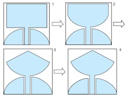
Rectangular patch antennas are typically known to provide narrowband characteristics. To improve the operating bandwidth, the authors shaped the bottom of the antenna patch into an arc. In practical applications, the size of ground plane is finite and the direction of maximum radiation tilts somewhat upward from the horizontal plane. To reduce this beam tilting, the ground plane of the proposed antenna was designed for a rounded rather than a rectangular shape. The arc-shaped patch and tapered ground plane make good broadband impedance matching of the antenna possible. To further expand the impedance bandwidth, several forms were etched from the patch: a right-angle triangle on the upper corners of the patch and a small fan angle on each side of the ground plane near the feed line.16 These improvements are highlighted in Fig. 1.
1. These steps show the process of improving a patch antenna with built-in notches.
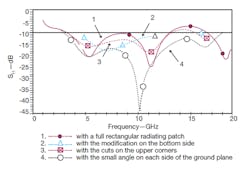
Figure 2 shows a comparison of the simulated reflection coefficient (S11) for an antenna with full rectangular radiating patch with an antenna modified on the bottom—with cuts on the upper corners and the small angle on each side of the ground plane—when all the dimensions are the same. The first line demonstrates the rectangular patch antenna has a narrowband characteristic. The second line shows the impedance bandwidth is broadened when the bottom of the patch is shaped into an arc. On the basis of this, the third line about the upper corners modification indicates that the bandwidth has been further expanded compared with the second line (the main advantages that this modification is reducing the lowest frequency). The fourth line demonstrates the small angle on each side of the ground plane near the feed line will affect the characteristic impedance of the CPW line and also contribute to the modified antenna’s very wide impedance bandwidth.16
2. These curves represent simulated reflection coefficients for different shapes of the radiation patch and the ground plane.
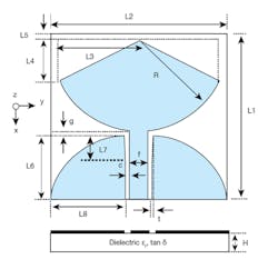
Figure 3 shows the final geometry of the proposed antenna (referred to as antenna A),16 which was measured 28 x 30 mm printed on FR-4 substrate. The circuit-board material has 1.6-mm thickness, relative permittivity of 4.4, and loss tangent (tan δ) of 0.02. The antenna is formed in the x-y plane with normal direction parallel to the z-axis. The center strip and gap of the CPW line are 3.6 and 0.3 mm, respectively, to achieve a 50-Ω characteristic port impedance. The improvement steps mentioned earlier contribute to good impedance matching across a wide bandwidth.
3. This diagram shows the configuration of proposed antenna A.
The antenna’s geometric parameters were optimized for S11 ≤ −10 dB across the full frequency range using ANSYS HFSS 11.0 electromagnetic (EM) simulation software from Ansys. The final antenna geometry parameters were obtained as L1 = 28 mm, L2 = 30 mm, L3 = 13.5 mm, L4 = 5 mm, L5 = 1.5 mm, L6 = 10.8 mm, L7 = 5.4 mm, L8 = 12.9 mm, R = 15 mm, g = 0.7 mm, f = 3.6 mm, c = 0.3 mm, t = 0.3 mm, and H = 1.6 mm. By selecting optimal parameters, the proposed antenna can be tuned to operate across the UWB band.
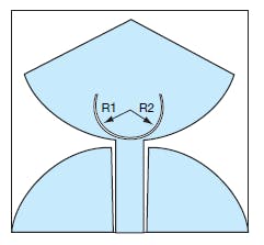
Since UWB radios share part of the spectrum with HIPERLAN/2 applications (5.15 to 5.35 GHz and 5.470 to 5.725 GHz) and WLAN applications using the IEEE 802.1la protocol (5.15 to 5.35 GHz and 5.725 to 5.825 GHz), an UWB antenna with reconfigurable band-rejection characteristic at WLAN frequencies is highly desirable. Several designs of UWB antennas with band-rejection characteristics have been investigated and successfully implemented in the past. The simple and commonly used approach is to incorporate slots into the antennas’ main radiator. Figure 4 shows a schematic diagram of the UWB planar antenna (referred to as antenna B) with filtering property operating in the 5-to-6-GHz band.
4. This diagram shows the configuration of proposed antenna B.
Band-notched operation is achieved by using a C-shaped slot in the radiating patch of antenna A. When the band-notched design was applied to antenna A, no retuning work was required for the previously determined dimensions. A simple relationship shows the notch frequency (fnotch) for the dimensions of the band-notch feature:
fnotch = c/[2L(εeff)0.5] (1)
where:
L = the total length of the C-shaped slot;
εeff = the effective dielectric constant of the substrate; and
c = the speed of light in free space.
In this design, the C-shaped slot was chosen to be nonresponsive close to about 0.33λ at the center frequency of the desired notched-band, where λ is the wavelength at the center frequency of the rejection band. The final design parameters of the C-shaped slot were chosen to be R1 = 4.3 mm and R2 = 4.5 mm.
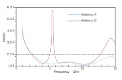
Figure 5 plots simulated VSWR for the antenna, illustrating that a sharp stopband is possible by inserting a C-shaped slot in the antenna’s radiating patch. Compared to antenna A, this single band-notched UWB antenna (antenna B) successfully blocks out the 5-to-6-GHz band while maintaining good impedance matching at other frequencies across the UWB band.
5. These curves compare the simulated VSWRs of antennas A and B.
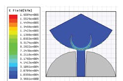
Figure 6 shows the current distribution around the slot of antenna B at the 5.5-GHz notch frequency. At 5.5 GHz, the current flows mainly around the C-shaped slot. The impedance is nearly zero at the top of the slot and the impedance is very high near the antenna feed line. In this case, the high impedance at the feed point leads to the desired impedance mismatch near the 5.5-GHz notch frequency.
6. This diagram simulates current distributions at 5.5 GHz for antenna B.
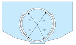
In addition to WLAN systems, WiMAX (3.3 to 3.6 GHz) and C-band communications systems (3.7 to 4.2 GHz) may interfere with UWB communications systems, prompting the need for antennas with multiple notched bands. Antennas with dual notched bands can be realized by using two nested C-shaped slots in the radiating patch (antenna A), which can yield band-notched characteristics centered at 3.4 and 5.5 GHz, respectively. Figure 7 shows the geometry of the UWB antenna (referred to as antenna C) with dual notched-band characteristics. Since mutual coupling exists between the exterior and interior C-shaped slots, the HFSS simulated values did not match the predicted values. The optimized design parameters are R1 =4.5 mm, R2 = 4.2 mm, R3 = 4.0 mm, and R4 = 3.7 mm.
7. This is the physical configuration of proposed antenna C.
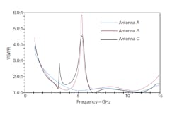
Figure 8 shows simulated VSWR as a function of frequency for proposed antenna C. Results of the reference antennas without band-notched characteristics and with single band-notched characteristic are also shown for comparison. Antenna C, with its two notched bands, exhibits notched bands of 3.3 to 3.6 and 5 to 6 GHz, while maintaining wideband performance from 2.2 to 13 GHz for VSWR ≤ 2.0:1, covering the entire UWB frequency range.
8. These curves compare the simulated VSWRs of antennas A, B, and C.
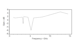
The proposed antenna design features two strong notched bands, created by the two nested C-shaped slots. Figure 9 shows simulated gain. As expected, sharp gain decreases occur in both the 3.3-to-3.6-GHz and 5-to-6-GHz bands. However, for other frequencies outside the rejected bands, the antenna gain is nearly constant across the entire UWB band.
9. This plot shows the simulated gain of proposed antenna C.
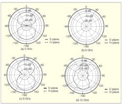
Figure 10 shows the simulated radiation patterns for the proposed antenna, at 3 GHz, 6 GHz, 9 GHz and 12 GHz for E- and H-plane patterns. The greatly distorted radiation pattern at 12 GHz [Fig. 10(d)] is caused by seriously unequal phase distribution on the antenna aperture and increased magnitudes of higher-order modes. The four plots show the radiation plots of antenna C; the radiation patterns of antenna A and antenna B are not depicted. From the analysis presented in ref. 12, these proposed band-notch structures have minimal influence on the radiation patterns of an UWB antenna.
10. These H- and E-plane radiation patterns were made at (a) 3 GHz, (b) 6 GHz, (c) 9 GHz, and (d) 12 GHz.
In summary, the structural modifications detailed for patch antennas successfully achieve sharp notches where needed across the frequency ranges of UWB antennas. As was shown, by inserting two nested C-shaped slots in the radiating patch, notches of 3.3 to 3.6 GHz and 5 to 6 GHz (representing WiMAX and WLAN frequencies, respectively) can be obtained. Owing to the simple structure and ease of impedance matching, the proposed antennas should be profitable for multiband applications.
Jie Jin, Doctor
Fei Yu, Doctor
College of Information Science and Engineering, Jishou University, Jishou416000, People’s Republic of China; e-mail (Jie Jin): [email protected], (Fei Yu): [email protected]
References
1. First report and order in the matter of revision of Part 15 of the Federal Communication Commission’s rules regarding ultra-wideband transmission systems, FCC (www.fcc.gov), ET-Docket 98-153, 2002.
2. F. Yu and C.-H. Wang, “Tiny antenna arms UWB applications, Microwaves & RF, Vol. 49, No. 13, 2010, pp. 54-60.
3. A. Mehdipour, K. Mohammadpour-Aghdam, R. Faraji-Dana, and M.-R. Kashani-Khatib, “A Novel Coplanar Waveguide-Fed Slot Antenna for Ultrawideband Applications,” IEEE Transactions on Antennas and Propagation, Vol. 56, No. 12, 2008, pp. 3857-3862.
4. K.-S. Ryu and A.-A. Kishk, “UWB Antenna With Single or Dual Band-Notches for Lower WLAN Band and Upper WLAN Band, ” IEEE Transactions on Antennas and Propagation, Vol. 57, No. 12, 2009, pp. 3942-3950.
5. M. Ojaroudi, C. Ghobadi, and J. Nourinia, “Small Square Monopole Antenna With Inverted T-Shaped Notch in the Ground Plane for UWB Application,” IEEE Antennas and Wireless Propagation Letters, Vol. 8, 2009, pp. 728-731.
6. S. Nikolaou, N.-D. Kingsley, G.-E. Ponchak, J. Papapolymerou, and M.-M. Tentzeris, “UWB Elliptical Monopoles With A Reconfigurable Band Notch Using MEMS Switches Actuated Without Bias Lines,” IEEE Transactions on Antennas & Propagation, Vol. 57, No. 8, 2009, pp. 2242-2251.
7. W.-T. Li, X.-W. Shi, and Y.-Q. Hei, “Novel Planar UWB Monopole Antenna With Triple Band-Notched Characteristics,” IEEE Antennas and Wireless Propagation Letters, Vol. 8, 2009, pp. 1094-1098.
8. Y.-J. Dong, W. Hong, Z.-Q. Kuai, and J.-X. Chen, “Analysis of Planar Ultrawideband Antennas With On-Ground Slot Band-Notched Structures,” IEEE Transactions on Antennas and Propagation, Vol. 57, No. 7, 2009, pp. 1886-1893.
9. K. Chung, J. Kim, and J. Choi, “Wideband microstrip-fed monopole antenna having frequency band-notch function,” IEEE Microwave and Wireless Components Letters, Vol. 15, No. 11, 2005, pp. 766-768.
10. F. Yu and C.A. Wang, “A CPW-Fed Novel Planar Ultra-Wideband Antenna with a Band-Notch Characteristic,” Radioengineering, Vol. 18, No. 4, 2009, pp. 551-555.
11. Y. Kim and D.-H. Kwon, “CPW-fed planar ultra wideband antenna having a frequency band notch function,” Electronics Letters, Vol. 40, No. 7, 2004, pp. 403-405.
12. Q.-X. Chu and Y.-Y. Yang, “A Compact Ultrawideband Antenna With 3.4/5.5 GHz Dual Band-Notched Characteristics,” IEEE Transactions on Antennas and Propagation, Vol. 56, No. 12, 2008, pp. 3637-3644.
13. Y.-S. Li, Y.-D. Yang, and Y. Bai, “Tiny UWB antenna notches two bands,” Microwaves & RF, Vol, 51, No. 2, February 2012, pp. 81-84.
14. H.-J. Zhou, B.-H. Sun, Q.-Z. Liu, and J.-Y. Deng, “Implementation and investigation of U-shaped aperture UWB antenna with dual band-notched characteristics,” Electronics Letters, Vol. 44, No. 24, 2008, pp. 1387-1388.
15. C.-Y. Huang C.-Y., C.-C. Lin, and W.-F. Chen, “Multiple band-stop bow-tie slot antennas for multiband
wireless systems,” IET Microwaves Antennas & Propagation, Vol. 2, No. 6, 2008, pp. 588-593.
16. M.-A. Matin, “Ultra Wideband Communications: Novel Trends—Antennas and Propagation,” InTech Open Access Publisher, Croatia: Rijeka, 2011, pp. 239-254.
