A Practical Design Approach to Custom mmWave SMT Packages
Download this article in PDF format.
After many years of research and development, electrical engineers, physicists, mathematicians, and scientists have come to realize the benefits of operating communications systems at higher frequencies. Some of the most notable advances stemming from this research include smaller circuit implementations for the same functionality, improved antenna gain for a given antenna size, and dramatic increases in data-carrying capacity. However, numerous challenges remain in implementing high-frequency circuits under real-world constraints. Among the non-trivial problems, packaging is one that stands out.
It’s critical that packages for RF components allow for the integration of multiple circuital technologies while achieving the best possible balance of performance and cost for a given application. Nevertheless, traditional packaging techniques have proven incapable of translating the same performance typically seen below X-band into the millimeter-wave (mmWave) range due to embedded parasitics and other inherent technological constraints. These limitations have led the design community to leverage the latest packaging technologies, novel design methodologies, and advanced CAD tools to develop cost-effective, scalable packaging solutions for high-frequency markets and applications.
These new packaging techniques are now moving away from performance-degrading implementations, such as molding compounds and long wire-bonding structures, to achieve outstanding performance beyond 55 GHz. In light of these developments, this article explores some of the key concepts that underlie the development of commercially viable packaging solutions for mmWave components (patent pending).
Introduction
Global mobile data usage is expected to grow from 11.2 petabytes/month in 2017 to 48.3 petabytes/month in 2021. 5G has emerged as a strong proposal to increase mobile data capacity by a factor of 1000 and support the expected data consumption of seven billion people and seven trillion devices. All of this would happen while still retaining energy efficiency and maintaining near-zero downtime.1
The advent of 5G has brought about an increase in development of integrated circuits (ICs) to meet the requirements for high-frequency applications. The need also arises for the development of cost-effective packages that not only protect the ICs, but are also capable of maintaining good electrical performance across wide operational frequency bands.
Current surface-mount quad-flat no-leads (QFN) packages are not suitable for packaging devices at mmWave frequencies. Parasitic elements encountered in the signal path—for example, discontinuities in the vertical transition from the printed circuit board (PCB) to the top side of the QFN and from the wire bond to the IC—are negligible at lower frequencies. However, such discontinuities become relevant once the physical dimensions of the elements become a fraction of the wavelength.
Another drawback associated with QFN packages is their reliance on over-molding. This not only increases electrical loss at higher frequencies, but also makes it impossible to package die featuring air bridges. Moreover, QFN packages are incapable of accommodating flip-chip devices due to their standardized nature.
Many solutions have emerged to address these challenges. Air-cavity QFN packages allow for ICs with air bridges, but they still lack a well-matched transition at high frequencies. Micro-Coax structures allow for high-frequency operation but require specialized assembly processes.2 Custom packaging solutions can compensate for parasitic effects and allow for air-cavity implementation.3 Fully-custom solutions are most viable when incorporated into a rapid, low-risk design strategy as well as a highly automated assembly process.
Modern RF applications have stringent requirements for components beyond electrical specifications. Dense assemblies, high operating powers, and the need for robust, reliable systems place heavy demands on monolithic-microwave-integrated-circuit (MMIC) package designers in terms of balancing electrical performance with desirable thermal and mechanical characteristics.
Since design features that benefit one aspect of performance may detract from the requirements of others, tradeoffs are often necessary. For example, a tradeoff intended to improve electrical performance at the expense of heat dissipation may produce little benefit due to a temperature rise on conductors and semiconductors. It’s therefore critical for designers to understand the simultaneous effects of design choices on the different aspects of a device’s performance.
In this article, we present the development of custom surface-mount packages with good electrical performance from dc to 50 GHz, accounting for the PCB, the surface-mount package, and the IC (patent pending). What follows is a discussion of the package’s components and design. After that, the article dives into the tradeoff between customization and standardization of design features in the context of performance and cost goals. Measured performance of a broadband MMIC attenuator die in both custom organic and low-temperature co-fired ceramics (LTCC) packages are shown. Also discussed are the benefits of a multi-physics simulation workflow employed in the design of these packages.
Design Elements
Structure
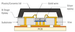
1. This is the schematical cross-section of a ceramic package.
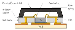
2. An organic package’s schematical cross-section is shown.
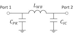
Schematical cross-section diagrams of the ceramic and organic packages with the PCB are shown in Figures 1 and 2, respectively. The description that follows is common to both. The IC is attached to the pocket inside the substrate using conductive epoxy. This implementation minimizes the length of the gold wire bonds. The gold wire connects the RF pads of the IC to the RF pads of the package, forming a lowpass network in which the wire bond is represented as a lumped series inductance, LWB, and the pads are represented as CPK and CIC (Fig. 3).
3. Here’s a lumped-element representation of the gold wire interconnect between the package pad (CPK), the gold wire (LWB), and the IC pad (CIC).
Proper tuning of this matching network is critical for an accurate impedance match and good wideband electrical performance. The package’s RF pad is followed by a microstrip line with 50-Ω characteristic impedance, and a matched vertical transition down to the bottom pad. The bottom pad of the package is made to have a 50-Ω characteristic impedance in a grounded-coplanar-waveguide (GCPW) configuration. The package is soldered to the PCB, which employs GCPW with a 50-Ω characteristic impedance. A plastic or ceramic lid is attached to the package with a non-conductive B-staged epoxy.
Materials
Material and technology selection play a big role in the performance of a package. Selecting the right materials will depend on the application requirements, such as hermeticity, maximum operating frequency, package size, package weight, first- and second-level interconnects, thermal management constraints, and tolerable insertion loss of interconnects.4
In both the LTCC and organic substrate packages, the selection of substrate material must account for the dielectric constant and loss tangent needed to achieve the desired RF performance. The substrate also determines the package topology and the compatibility with the other materials.
The two substrates explored here are LTCC and organic substrate. The LTCC package consists of a ceramic monolithic structure with a cavity formed in the top tape layers of the substrate (Fig. 1, again). The exposed top face of the pocket features a continuous metallization that’s connected to the bottom ground pad through multiple vias. Being a stiffer material, it’s easier to wire bond.
In the case of the organic package, the pocket is created by removing a portion of the substrate and exposing the bottom metallization (Fig. 2, again). This allows for better RF grounding and thermal resistance.
In both packages, the conductor materials and finishes are selected to achieve good RF performance and to accommodate industry-standard assembly processes. The metal conductor on the LTCC package is typically silver with an electroless-nickel-immersion-gold (ENIG) surface finish. The plating protects the underlying silver from oxidation and must have properties compatible with soldering and wire-bonding processes.
The organic package employs copper conductors and may feature any of several different surface finishes. The choice of surface finish may be a critical matter in high-frequency applications, as both surface roughness and electrical conductivity have significant effects on insertion losses.5, 6
Selection of the conductive epoxy used to mount the MMIC die has a significant impact on the total thermal resistance of the package. As the main point of contact between the die and the package, the epoxy facilitates most of the die’s heat dissipation.
Simulation Workflow
During the design phase of this project, the electrical, thermal, and mechanical performance of the LTCC and organic packages were analyzed using a multi-physics simulation workflow. The simulation workflow employed multiple simulators that were operated sequentially, with each simulator’s results being used as part of the next simulator’s setup.
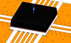
4. The electromagnetic simulation model of the LTCC package included only the design elements relevant to electrical performance.
The specific simulation workflow is as follows:
- A full 3D finite-element electromagnetic (EM) simulation is performed on a simplified version of the design’s geometry (Fig. 4). The simulation yields S-parameter data and a spatial distribution of power dissipation within the design.
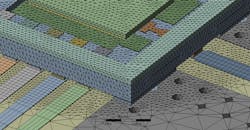
- A full 3D finite-element thermal simulation is run on the EM simulation’s model, augmented to include geometry relevant to thermal and mechanical (but not electrical) performance. As shown in Figure 5, effort was made to accurately model critical regions of simulation geometry, such as hollow and solder-filled plated through-holes (PTHs). The simulation employs the power dissipation computed from the EM simulation and yields a temperature distribution within the model’s geometry.
- A full 3D finite-element mechanical simulation is run on the full model geometry, employing the spatial temperature distribution as part of its setup. The simulation yields mechanical strains and stresses within the model geometry.
- If desired, the above process may be iterated until convergence criteria are met, feeding the temperature rise information and model geometry deformation into the electrical simulator for the next pass. In practice, a single pass is often sufficient to achieve outstanding agreement between simulation results and physical measurements.
5. This is a close-up of the geometry and mesh employed in thermal and mechanical simulations of the LTCC package with package lid hidden. Note that the model includes solder, die-attach epoxy, and both hollow and solder-filled plated through-holes.
While more complex than a workflow involving separate electrical, thermal, and mechanical simulation tasks, a true multi-physics simulation workflow gives design engineers a holistic view of a design’s performance. For example, a traditional thermal simulation of a microstrip conductor may involve a uniformly distributed heat source applied to the conductor’s volume or faces. Such an approach discards valuable information about localized heat generation, since current densities at mmWave frequencies are nonuniform. A multi-physics simulation approach implicitly captures this effect and others without needing attention from the designer.
The ability of a multi-physics simulation to automatically account for conditions too complex to manually set up is especially valuable for LTCC designs. As LTCC designs consist of a monolithic ceramic structure with complex internal conductor geometry, thermal images of the exterior of such a device may not fully reveal its internal thermal behavior.
Because the electrical, thermal, and mechanical aspects of a design’s performance are often linked (due to temperature-dependent electrical resistivities, thermal expansion, etc.), such a simulation workflow makes it possible to best understand the impact of design decisions on interrelated aspects of performance. The workflow has been qualified through multiple projects involving several technologies and achieves simulation results in very close agreement with performance measurements. As with other portions of Mini-Circuits’ established LTCC process, it’s subject to continual evaluation and improvement.
Customization vs. Standardization
Although the QFN package has been an industry workhorse for both active and passive electronic components up to V-band frequencies, its highly standardized nature makes it a suboptimal solution for some applications.7 As applications march toward mmWave frequencies, packaging technologies must adapt to widely varying industry needs.
While a one-size-fits-all solution may fit all applications equally poorly, a fully custom solution yielding outstanding results may be cost- and time-prohibitive. To develop a rapid, cost-effective packaging solution that still offers outstanding application flexibility, it was desirable to combine industry-standard processes and tunable design features into a customizable package template.
Taking a “templated” approach to package design allows for the reuse of proven design elements, reducing the effort and risk incurred by solutions that require starting from scratch. Facilities for adaptation to an application’s specific electrical, thermal, mechanical, and environmental needs are provided while minimizing or eliminating the need for extensive qualification of new designs.
QFN packages are typically available in a granular range of standardized sizes (3 × 3 mm, 4 × 4 mm, etc.), while a MMIC die may be any size and aspect ratio. A die that’s slightly too large to fit one standard QFN-package size must instead use the next size up, necessitating long wire bonds with correspondingly large parasitic inductances. The package itself offers little facility to compensate for these parasitics, a task relegated instead to conductor geometry on the PCB and die. Furthermore, QFN packages employ a plastic encapsulant that envelops the leadframe, die, and wire bonds.
Delicate structures on the MMIC die, like air bridges, are incompatible with such an encapsulation process. Even in the absence of incompatible MMIC features, the encapsulant may detune or degrade the performance of sensitive electronics simply by proximity. Finally, the terminals of the QFN package are highly standardized with little flexibility of the pad sizes and geometries. For some applications, the electrical parasitics associated with the fixed transition geometry may be unacceptable.
Mini-Circuits’ custom LTCC and organic substrate packages address the above limitations, offering solutions with sufficient flexibility to meet the needs of a wide variety of applications. In these packages, the die inhabits a pocket atop the substrate (Figs. 1 and 2, again). The pocket’s dimensions are specified according to the customer’s die so that wire-bond pads can be brought as close to the die as possible, minimizing bond-wire length and inductance.
Therefore, the LTCC and organic substrate packages offer greater flexibility with regard to MMIC die sizes, even though they are currently available in the same sizes as standard QFN packages (3 × 3 mm, 4 × 4 mm, and 5 × 5 mm). A plastic lid is affixed over the die and wire bonds with a B-staged epoxy compound, maintaining an air gap above the die and wire bonds and achieving a semi-hermetic seal. Using an air gap rather than an encapsulant permits the packaging of delicate MMIC structures and minimizes degradation of electrical performance.
Unlike QFN packages, the LTCC and organic substrate packages offer the flexibility needed to best suit a wide variety of applications. The package structure contains tunable elements that electrically compensate for the parasitics associated with the transitions from the PCB to the package and from the package to the MMIC die. Furthermore, since the package features printed conductors rather than a solid leadframe, the footprints of the LTCC and organic substrate packages can be customized with minimal tooling cost.
Examples
To validate the design and to measure the performance of the organic and LTCC packages, multiple packages were designed, fabricated, and tested. The packages were assembled and soldered on 5-mil Taconic TLY-5 evaluation PCBs with 50-Ω GCPW traces. Southwest Microwave 2.4-mm edge-launch connectors were used to interface the PCBs with the vector network analyzer (VNA). A standard short-open-load-thru (SOLT) calibration was performed up to 55 GHz, up to the reference plane of the connectors. The insertion-loss measurements for each package are normalized by subtracting the losses of the PCB thru-line.
MMIC 2-dB Attenuator on Organic Package
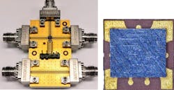
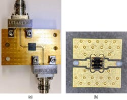
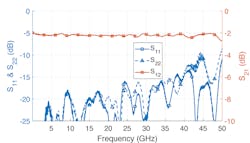
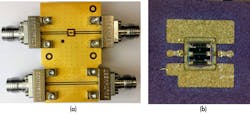
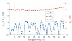
A 2-dB MMIC attenuator is mounted and wire-bonded on top of an organic package. Figure 6 shows the package mounted on top of the PCB, as well as a close-up of the package without the lid, depicting the die and the wire bonds. Figure 7 shows the measured data of the device. The S21 trace reveals a very flat response of −2 dB up to 48 GHz. A good return loss is also observed for the entire frequency bandwidth.
6. The IC in an organic package (with lid) is shown here on an evaluation board (a). A close-up of the package without the lid shows the flip-chip die atop package substrate (b).
7. These are the measurement results of a 2-dB attenuator on organic package.
MMIC 2-dB Attenuator on Ceramic Package
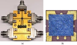
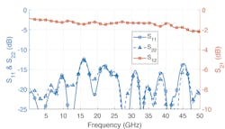
A 2-dB MMIC attenuator is mounted and wire-bonded on top of a ceramic package. Figure 8 shows the package mounted on top of the PCB, as well as a close-up of the package without the lid, illustrating the die and the wire bonds. Figure 9 shows the measured data of the device. The S21 trace reveals a very flat response of −2 dB up to 55 GHz. A good return loss is also observed for the entire frequency bandwidth.
8. Here, the IC is in an LTCC package on an evaluation board (a). A close-up of the package without the lid shows the die and wire bonds (b).
9. The plots reveal measurement results of a 2-dB attenuator on LTCC package.
Flip-Chip SPDT Switch on Ceramic Package
A flip-chip single-pole, double-throw (SPDT) switch is mounted on top of a ceramic package. Figure 10 shows the package mounted on top of the PCB, as well as a close-up of the package with the exposed flip-chip die. Figure 11 reveals the measured data of the device with the RF2 channel active. A good return loss is observed over the entire bandwidth.
10. Shown is the packaged IC on evaluation board (a). One can view a close-up of the package without the lid, showing die and wire bonds (b).
11. Measurement results indicate good return loss for the SPDT flip-chip switch with RF2 channel active.
Conclusion
Packages employing both LTCC and organic substrate materials have been developed (patent pending). Outstanding electrical performance of both packaging technologies was demonstrated up to 55 GHz. Both packaging methodologies accommodate a wide variety of application-specific needs, including impedance matching, variable die sizes, and a wide range of I/O pad counts, signal types (dc or RF), and PCB geometries. By combining standardized and adjustable features into a tunable package template, Mini-Circuits’ approach to packaging achieves desirable electrical performance and broad applicability while minimizing turnaround time, cost, and risk.
Acknowledgements
The authors would like to thank Mini-Circuits for providing the resources needed to conduct the research and develop the innovations presented in this article.
References
- National Instruments. (2018) 5G new radio: Introduction to the physical layer. [Online]. Available: http://www.ni.com/enus/innovations/wireless/5g/new-radio.html.
- E. A. Sanjuan and S. S. Cahill, “QFN-based millimeter wave packaging to 80ghz,” in 2009 IEEE MTT-S International Microwave Workshop Series on Signal Integrity and High-Speed Interconnects, pp. 9-1
- K. Fujii and H. Morkner, “Two novel broadband MMIC amplifiers in SMT package for 1 to 40 GHz low cost applications,” in 2005 European Microwave Conference, vol. 2, pp. 4 pp.–1086.
- R. Sturdivant, Microwave and Millimeter-Wave Electronic Packaging, ser. Artech House microwave library. Artech House, 2013. [Online]. Available: https://books.google.com.co/books?id=xphQAgAAQBAJ.
- J. Coonrod, “Ambiguous influences affecting insertion loss of microwave printed circuit boards [application notes],” IEEE microwave magazine, vol. 13, no. 5, pp. 66-75, 2012.
- M. Henry, C. Free, Q. Reynolds, S. Malkmus, and J. Wood, “LTCC technology at high millimeter wave frequencies,” in 2006 1st Electronic Systemintegration Technology Conference. IEEE, 200 [Online]. Available: https://doi.org/10.1109/estc.200280087.
- Mini-Circuits. (2018) EP2KA+ Datasheet. [Online]. Available: https://www.minicircuits.com/pdfs/EP2KA+.pdf.
