What’s the Difference Between GaN and GaAs?
Download this article in .PDF format
Gallium arsenide (GaAs) was once the automatic choice of semiconductor material for high-frequency solid-state devices, components, and integrated circuits (ICs), from amplifiers to switches.
As GaAs devices grew in popularity for RF/microwave applications, they rapidly replaced legacy silicon-based semiconductors, such as bipolar transistors and metal-oxide-semiconductor field-effect transistors (MOSFETs), which were limited in frequency compared to GaAs field-effect transistors (FETs), heterojunction bipolar transistors (HBTs), and high electron mobility transistors (HEMTs).
During the last decade, however, gallium nitride (GaN) has become the favorite high-frequency semiconductor compound, steadily replacing GaAs in many RF/microwave applications, especially where higher-frequency, higher-power semiconductors are required. But why the steady shift to GaN and just how different in performance are GaAs and GaN?
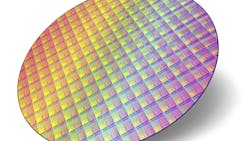
GaN and GaAs are both compound semiconductor materials, each composed of two elements. The materials are grown in the form of ingots, which are cut into thin wafers (see figure) upon which semiconductor devices, including passive circuit elements, are fabricated. GaAs is the more mature material and is commercially available in the form of wafers as large as 6 in. in diameter while GaN, which has been used to fabricate light-emitting diodes (LEDs) since the 1990s, is typically available in wafers as large as 2 in. in diameter.â
GaAs is well established as a substrate of choice for high-frequency, small-signal semiconductor devices, especially where low noise figure is needed, as in receiver front ends. GaAs monolithic microwave integrated circuits (MMICs) are widely used in portable wireless products, such as smartphones, tablets, and Wi-Fi devices. Components such as switches and amplifiers are typically incorporated into these GaAs MMICs, which are designed for operation at low voltages and currents typically available from a battery.
GaN, on the other hand, has come to be known as a power process, capable of fabricating active devices for amplifiers that can operate at voltages of +48 V dc and higher. With the higher-voltage capabilities of GaN devices and MMICs, they have become the active components of choice for such applications as power amplifiers in wireless base stations and have been steadily replacing high-frequency electron vacuum tubes in military radar and even in commercial and industrial microwave ovens. For a comparable output-power rating, GaAs amplifiers tend to be more linear, with less distortion, than GaN amplifiers, although GaN devices have been used with digital predistortion (DPD) to achieve enhanced linearity at higher frequencies.
Before attempting to compare differences in devices fabricated on the two high-frequency semiconductor materials, however, it is only necessary to assess the differences in characteristics of the two III-V compound semiconductors. These key material characteristics include relative dielectric constant (relative to the dielectric constant of a vacuum), breakdown voltage, electron mobility, saturation velocity, and thermal conductivity.

GaN is considered a wide-bandgap material compared to GaAs, with a bandgap of about 3.4 eV for GaN compared to 1.4 eV for GaAs. A material’s bandgap related to the amount of energy required to shift an electron from the top of the valence band to the bottom of the conduction band within a semiconductor formed on that material. A wide bandgap typically refers to a material with bandgap of greater than 1 or 2 eV.
GaN typically exceeds GaAs in material parameters relating to higher energy and power, and in the speed of achieving higher-energy states. For example, the saturation velocity of GaN, at 2.7 × 107 cm/s, is somewhat higher than the 2.0 × 107 cm/s of GaAs. The critical breakdown voltage field determines the highest voltage that can be safely applied to a solid-state device, and the breakdown electric field of GaN, at 4 × 10⁶ V/cm, is much higher than the 5 × 10⁵ V/cm of GaAs.
GaN has certain traits that support smaller circuits for a given frequency and power level, allowing the higher power densities and efficiencies much sought after by designers of power-efficient wireless base stations and microcells. For one thing, the higher-voltage capacities of GaN allow the fabrication of much smaller devices for a given power level than on GaAs materials. For example, the defect density of any semiconductor wafer will limit the practical size of circuits that can be manufactured repeatably and reliably on that wafer, implying that device area be minimized for best production yields.
Because the power density of GaN materials is much higher than GaAs or even silicon semiconductor materials, thermal conductivity is an important material parameter for characterizing how well a device will dissipate heat due to dielectric and conductor losses as well as basic device inefficiencies. The thermal conductivity of GaN, at 1.7 W/cm-K, is more than three times the thermal conductivity of GaAs, at 0.46 W/cm-K. High thermal conductivity translates into the lowest temperature rise at conduction, a characteristic that enables GaN devices to handle higher power levels than GaAs devices using the same device structure, such as a field-effect transistor (FET).
GaN devices are currently fabricated on different substrate materials, such as GaN on silicon (Si) and GaN on silicon carbide (SiC) wafers, with some debate about which process offers the best performance. Some larger companies, such as Raytheon Co., maintain both GaAs and GaN foundries as part of their in-house capabilities in support of military applications. Many commercial foundries will offer details on the benefits of each process with some foundries, including WIN Semiconductors Corp., Global Communication Semiconductors LLC, and Qorvo, offering different forms of GaN processes along with GaAs fabrication services as well.
For those wishing a finer-grained comparison of GaN and GaAs materials, MACOM, with products based on more than a half-dozen semiconductor processes, offers a detailed comparison of the different semiconductor materials on their website.
Looking for parts? Go to SourceESB.
About the Author
Jack Browne
Technical Contributor
Jack Browne, Technical Contributor, has worked in technical publishing for over 30 years. He managed the content and production of three technical journals while at the American Institute of Physics, including Medical Physics and the Journal of Vacuum Science & Technology. He has been a Publisher and Editor for Penton Media, started the firm’s Wireless Symposium & Exhibition trade show in 1993, and currently serves as Technical Contributor for that company's Microwaves & RF magazine. Browne, who holds a BS in Mathematics from City College of New York and BA degrees in English and Philosophy from Fordham University, is a member of the IEEE.
