X-band Push-Push Oscillator Simulation and Measurement (Part 2)
Download this article in PDF format.
This article continues where Part 1 left off with a discussion of the push-push oscillator topology. The push-push oscillator circuit topology joins two common-collector oscillators at the grounded end of the resonator (Fig. 1). The voltage null of each section of the oscillator becomes the common junction of the push-push configuration, and the coupled transmission line is removed in favor of a simple coupling capacitor.
1. This is the push-push oscillator circuit topology. The push-push oscillator is structured from the connection of two common-collector oscillators such that the null point of the circuit is maintained.
For a voltage null to exist at the junction of the oscillator sections, each oscillator must generate a signal that’s coherent and in phase opposition. Clearly, symmetry and circuit balance are requirements for quality push-push oscillator operation. The second harmonic of the oscillator sections is extracted at the null point while the fundamental is cancelled. The primary frequency acts as an idler to produce an output signal with significant second-harmonic content. This is accomplished principally because the fundamental signal component isn’t loaded. Therefore, highly nonlinear operation is assured.
Although the grounded collector oscillator has been selected, it should be emphasized that other oscillator configurations are applicable—in fact, other types of devices are applicable. The principal criterion is that a negative resistance is required, as is a means of joining the negative resistance devices in a manner that ensures synchronization and out-of-phase signal generation from each device.
Simulation Technique
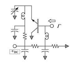
The bipolar junction transistor (AT42000) is initially investigated under small- and large-signal conditions using the feedback capacitor to maximize the reflection coefficient over the anticipated bandwidth of the oscillator. This investigation is conducted using the schematic shown in Figure 2, in which the device is biased at a nominal operating point and a signal is applied to the negative resistance port at variable power levels.
2. Initial negative resistance investigation is conducted using this schematic. The reflection coefficient is optimized with the feedback capacitor and plotted as the input power is increased.
After optimization of the reflection coefficient at the base under small-signal conditions using the variable feedback capacitor, the reflection coefficient is repeatedly measured under increasing input RF power conditions.
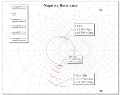
As may be readily discerned from Figure 3, the reflection coefficient decreases as the signal level increases, as one might expect from an intuitive understanding regarding the signal limiting of oscillators. Note that the negative resistance decreases with increasing RF input power. This is expected and mirrors the phenomenon that occurs as the oscillator starts and settles to the final operational conditions.
3. Large-signal reflection coefficient is compared with drive power. Note that the large-signal reflection coefficient decreases as input power is increased. This observation validates oscillator theory with respect to the buildup of signal to the steady-state limiting—the net oscillator loop resistance is zero at steady state.
Such an exercise may also be used to predict oscillation frequency—for example, continue to increase the signal level and observe the point where the reflection coefficient magnitude is equal to unity. At this point, one may read the real and imaginary parts of the impedance. The reflected impedance from the coupled resonator is also illustrated. The point at which the negative resistance at the base of the transistor is equal to the coupled port positive resistance and the total loop reactance cancels is the oscillation frequency.
This is an estimate and most large-signal simulation algorithms are much more sophisticated in both technique and execution. However, it’s instructive to observe the behavior and validate the traditional understanding of oscillator theory.
It’s also instructive at this point to alter the feedback capacitance to ensure that the maximum reflection coefficient is maintained at the base of the transistor. To ensure that the oscillator starts under small-signal conditions is the first requisite; to maintain a healthy oscillator, the feedback capacitor must also sustain the large-signal limiting conditions. A phenomenon that’s been observed is the oscillation cycle of start, saturation, and subsequent quenching.
The common-collector oscillator was further explored using the coupled transmission line as a parametric variable. The parameters of output power, phase noise, and load line were documented for various coupling values.
Simulation Results
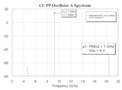
The simulation algorithm begins with a frequency search of the required conditions for oscillation under small-signal conditions. It proceeds to find a large-signal, steady-state solution at the identified spectral areas using a probe element as described in Appendix B. Figures 4, 5, 6, 7, 8, and 9 reveal the simulation data.
4. The spectral content at Vt = 4.0 V dc shows the strong second harmonic as expected with fundamental, third-, and fourth-harmonic levels present.
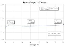
5. Shown is power output versus tune voltage. The oscillator power output remains constant within 0.25 dB over a voltage tuning range of 8 V.
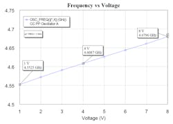
6. The oscillator output frequency (fundamental) versus tuning voltage discloses 250 MHz of voltage tuning over 8.0 V. The tuning range is a strong function of the varactor coupling capacitors. A tuning range of 1.0 GHz has been noted with larger coupling capacitors.
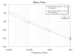
7. Shown is phase noise versus offset frequency of the push-push oscillator and the single common-collector oscillator. Because one expects a 6-dB difference, some noise suppression is indicated. Phase noise of −100 dBc/Hz has been measured on the push-push configuration, indicating excellent correlation.
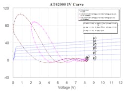
8. The dynamic load line of the push-push oscillator and the single common-collector oscillator discloses profound nonlinear operation of the push-push oscillator. Operation at high collector current and low collector voltage has been correlated with poor phase noise.
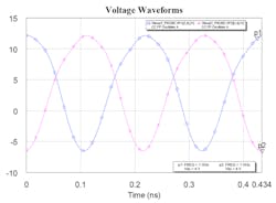
9. Shown are the voltage waveforms at the base of the push-push stages, which disclose the out-of-phase signals as expected.
J.M. Ziman once said, “It is typical of modern physicists that they will erect skyscrapers of theory upon the slender foundations of outrageously simplified models.” Like the modern physicist, the engineer should be cautious in the use of overly simplified models.
Prediction of Oscillator Center Frequency
The simulation utilized a published Spice model of the AT420 bipolar transistor. Attempts to validate the model from the manufacturer were not successful. In fact, S-parameter data did not correlate well between the manufacturer’s published data and S-parameters simulated with the Spice model. This lack of correlation is believed to be responsible for the poor correlation between the measured (10 GHz) and simulated center frequency (9.2 GHz).
Prediction of Oscillator Phase Noise
The measured oscillator phase noise was −45, −73, and −100 dBc/Hz at the respective offset frequencies of 1, 10, and 100 kHz. The simulated phase-noise data is −61, −84, and −104 dBc/Hz at the respective offset frequencies. Phase noise of a free-running oscillator near to the carrier is closely related to the Spice model noise parameters. Unfortunately, Spice noise parameters are generally not published and when published, disclaimers sometimes follow with respect to production lot variations and measurement methods.
The Spice noise parameters—AF, KF, and FFE—for the AT420 transistor are not available from the manufacturer. Therefore, the author relied on measured data from Gris.1 The deviation between measured and simulated phase noise was not unexpected.
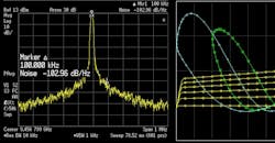
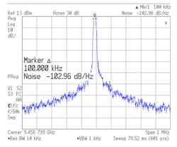
Measurements of a second push-push oscillator disclosed better correlation (Fig. 10).
10. This is the phase noise of the prototype push-push oscillator.
Prediction of Oscillator Output Power
The measured oscillator output power included a saturated buffer amplifier. Therefore, correlation between simulated output power could not be immediately determined.
Prediction of Oscillator Voltage Tuning
The oscillator frequency versus voltage tuning was 250 MHz (simulated) compared to 575 MHz (measured) for the push-push prototype. Clearly, further investigation is required. The oscillator tuning versus voltage relies on the varactor model and the coupling capacitor. The hyper-abrupt tuning varactor part number is MHV514-21, from Micrometrics. Micrometrics supplied the Gamma and capacitance versus voltage data.
The data was entered into the simulation as discrete points and a polynomial regression was used within the program to approximate a continuous function. An error tolerance may be specified to indicate if the polynomial deviates from the discrete point data by more than a specified percent. In this case, the error was less than 2%.
Oscillator Simulation Issues
Simulation of RF/microwave oscillators presents several limitations with respect to accuracy, particularly under conditions in which the active device operates over a wide dynamic range of current and/or voltage. More specifically, bipolar-junction- and field-effect-transistor (BJT and FET, respectively) noise parameters vary dramatically with bias, and unfortunately, are usually extracted under “nominal” bias conditions.
While parametric extraction at “nominal” bias conditions is quite adequate for small-signal and some large-signal amplifier simulations, it’s entirely inadequate for accurate oscillator simulation. An additional consideration is the statistical variation of parametric device data typically associated with manufacturing processes and other tangential considerations, i.e., environment.
Notwithstanding the benefits and improvements in harmonic-balance simulation algorithms, accurate oscillator simulation requires parametric data of the active device over the entire range of operational current and voltage. The extraction of a single set of parameters to represent the active device under static and dynamic operation is a formidable task.
From experience with the push-push oscillator of this investigation and other less-complex oscillator circuit topologies, the fundamental limitations in simulation accuracy are summarized:
- Inaccurate BJT and FET device model parameters and parameter variation; particularly noise parameters
- Resistive and reactive loading of the fundamental and harmonics
- Highly nonlinear device operation, i.e., see the dynamic load-line excursion
- Device manufacturing variance
In addition to accurate model data over large regions of the operating voltage and current, i.e., cutoff to saturation, harmonic-balance algorithms exhibit a profound impact in oscillator simulation performance.
Conclusions
Conventional oscillator theory of operation has been demonstrated using a simple common-collector oscillator configuration. The common-collector oscillator has been extended and shown to be a basic element of the push-push oscillator circuit topology. Highly nonlinear operation, model device parameter extraction, and simulation algorithm are fundamental limitations to accurate oscillator simulation. Notwithstanding accuracy limitations, computer simulation is shown to be an effective educational tool.
The 2019 Perspective
As mentioned in Part 1, this technical documentation was originally written in 2005 to address oscillator tuning issues within a radar subsystem. The exercise created a better understanding of the push-push oscillator circuit topology, and to that extent, the simulation software provided a valuable contribution, notwithstanding the BJT device model limitations.
In retrospect, several elements merit consideration:
- The active device model remains a significant issue with respect to simulation accuracy, particularly phase-noise prediction.
- The Spice model selection remains an appropriate choice for oscillator simulation.
- Discrete BJT and FET oscillator design is becoming—or has become—the province of MMIC manufacturers. Over the last 15 years, the author’s oscillator design activities have entailed MMIC device selection, i.e., VCOs, PLLs, and transmit/receive subsystems.
- The unique low-phase-noise property of the push-push oscillator circuit topology is likely the higher quality factor (Q) due to reduced loading at the fundamental frequency, as suggested by Gris1 and coupled oscillator properties as described in Chang5 (the Chang reference has been added to the 2019 revision).
- The dynamic load line is an effective indication of the degree of nonlinear operation and may be useful in assessing negative resistance and resonator loading.
- The simulation utilized the same common-collector elements. An interesting investigation would encompass intentional asymmetry to disclose performance variations.
- An interesting investigation—and one that the author intends to explore—is the addition of devices to the push-push topology. The performance expectation is increased power output and lower phase noise.
Appendix A
Oscillator Simulation using the Probe Element (see footnote 1 at end of article)
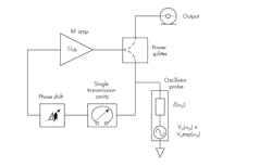
The oscillator probe element is a popular technique used in large-signal simulation of oscillators. To understand the operation and simulation algorithm, consider Figure A-1 in which a typical feedback oscillator is shown with the probe element connected to a resonator located within the feedback loop.
A-1. This is a feedback oscillator with probe element.
The probe element has the following properties:
- Presents a short circuit at the source frequency and an open circuit elsewhere.
- Probe voltage and frequency are adjusted to exactly equal the steady-state operating voltage.
- No current flows through the probe at the probe frequency or any other harmonic.
The probe frequency and amplitude are scanned in a search algorithm that identifies the signal frequency and amplitude at the connection point of the probe. When the signal frequency and amplitude are identified at the connection node, the probe no longer disturbs the circuit. Also, its frequency equals the oscillation frequency while its amplitude equals the amplitude at the node to which the oscillator probe is connected. Oscillator analysis is reduced to standard harmonic-balance analysis running in the inner loop of a routine that attempts to locate probe parameters (amplitude and frequency), which result in zero current flow through the probe’s terminals.
In negative-resistance oscillators, the probe should be connected between the resonator and the negative resistance-generating active device. In feedback oscillators, the probe should be connected to one of the nodes belonging to the feedback loop. Other connections of the oscillator probe generally result in excessive time to achieve convergence of the harmonic simulation algorithm as well as decrease accuracy. Sometimes, an alternate connection will fail to predict oscillation in an otherwise properly operating circuit.
The author has found rapid convergence and frequency prediction when the probe element is connected to the frequency-determining element of the oscillator circuit. While this has not been analytically verified, it’s suspected that the slope of the reactive impedance at the node of the probe is a component of the search algorithm.
Appendix B
Oscillator Simulation using the Test Element (see footnote 2 at end of article)
The oscillator test element is used to determine loop gain in oscillator design under large-signal conditions.
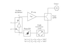
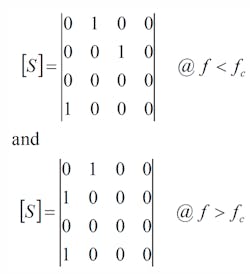
Referring to Figure B-1, large-signal excitation is applied to port 3. The large-signal S-parameter, S21, at the fundamental frequency is monitored. The cutoff frequency, fc, must be set to any value between the fundamental frequency and the second harmonic. When the excitation is weak, |S21| must be greater than unity to ensure that the start conditions are satisfied. As the excitation level is increased, |S21| decreases as the circuit enters saturation.
B-1. This diagram depicts a feedback oscillator with test element.
At some frequency and some excitation level, |S21| = 1 and its phase is zero. This point corresponds to the oscillation frequency. The output power under these conditions is the oscillator's output power. This operational procedure is and has been experimentally verified.
Before the oscillator test element can be used under large-signal conditions, it’s best to make an initial small-signal design of the oscillator. The circuit should be adjusted so that |S21| > 1 and the phase is zero under small-signal conditions at the desired frequency of oscillation. Increasing the excitation changes the frequency of zero phase shift, and thus it may be necessary to "tweak" the design to keep it on the right frequency. One would expect this phenomenon simply because the active device parameters change with signal level.
The oscillator test element permits the total loop gain to be measured under small- and large-signal conditions and evaluated without disturbing the circuit operation. It’s especially useful in analysis of oscillators with discrete feedback loops. An additional feature of the oscillator test element is the determination of frequency control using the phase-shift element. This is accomplished via measurement of large-signal magnitude of S21 while varying the phase shift. The oscillator tuning range is determined by observing the frequency points at which large-signal S21 is less than unity.
The S-parameters of the oscillator test element (Fig. B-2) are similar to those of a three-port isolator. They permit circuit excitation without altering circuit function for the measurement of closed-loop gain and phase.
B-2. The oscillator test element S-parameters resemble that of a three-port isolator.
Valid large-signal models of active devices are essential for accurate oscillator simulation.
Footnotes
1. The oscillator probe element, which initiates a large-signal oscillator simulation, is an ideal source in series with an ideal impedance element. The impedance presents an open circuit at all frequencies other than the fundamental frequency of oscillation. Source: Help resource, AWR Design Environment v14.03 Edition.
2. The oscillator test element is used to determine loop gain in oscillator design and break the feedback loop of an oscillator in the forward direction at the fundamental frequency. When this is done, a source at port 3 is used to replace the feedback signal and the feedback itself is measured at port 4. As a result, one can determine the open-loop gain of the circuit under large-signal conditions. Source: Help resource, AWR Design Environment v14.03 Edition.
References
- Gris, M., “Wideband, Low Phase Noise Push-Push Oscillator,” Applied Microwave and Wireless, January 2000.
- Yabuki, Sagawa, and Makimoto, “VCOs for Mobile Communications,” Applied Microwave and Wireless, Winter, 1991/199
- Scherer, D., “Low Phase Noise Design Tutorial,” HP Measurement Symposium, October 1978.
- AWR Microwave Office User Manual, version 5.53.
- Chang, Cao, Mishra, York, “Phase Noise in Coupled Oscillators: Theory and Experiment,” IEEE Trans. MTT, Vol. 45, No. 5, May 1997.
