Noise Sources in Ultra-Low-Noise Synthesizer Design
Series: Ultra-Low-Noise Synthesizer Design
Download this article in PDF format.
Phase noise is an interference source and a dynamic range limit in communications systems. The noise can cause interference both “in-channel” for systems with modulation terms close to the carrier, or further from the channel being used in what’s often referred to as adjacent or alternate channel performance.
As communications systems are often expected to operate under large link loss conditions, often exceeding 130 dB and sometimes exceeding 150 dB, it’s necessary for them to have a low noise floor, sometimes at the limit of the physically possible. Deliberately designing for this particular kind of noise control is not often taught in electrical engineering curricula, even at the graduate level. Also, in recent years, the technology of synthesizer design has changed dramatically, with noise control becoming more based on in-loop bandwidth suppression of voltage-controlled oscillator (VCO) noise, allowing noisier on-die VCOs to still deliver excellent performance. This noise suppression is particularly important with the high loop bandwidths enabled by modern sigma-delta synthesizer ICs using the latest high-frequency, low-noise crystal reference oscillators.
This article is the second, moderately longer online version in our low-noise synthesizer design series. A still more complete version will be posted on the Publications page at www.longwingtech.com. The first article (Ref. 1) covered basic design for functionality and stability. This second article, as well as the upcoming Part 3, will extend the basic methods to specifically cover designing for minimum phase noise. It focuses on noise sources outside the synthesizer integrated circuit (IC), such as the VCO and the various loop-filter forms.
The synthesizer IC noise and loop functions for shaping and combining all of the sources will be presented in the next article, revealing how modern synthesizer ICs with on-die VCOs can deliver performance that’s often competitive and sometimes superior to synthesizers with low-noise discrete VCOs. The fourth article in this series will cover parts and CAD tools available to the low-noise synthesizer designer, including the latest synthesizer ICs, crystal references, op amps, and VCOs that enable the very lowest noise designs. The fifth and final article will bring this material together in the form of low-noise synthesizer examples.
Frequency-Domain Definition of Phase Noise
We may think of phase noise as the frequency-domain spectral-density noise surrounding the carrier of a frequency source such as a VCO. Phase noise is mostly in the form of phase variation in a compressed oscillator, which will consist of the oscillator’s own noise as well as terms from the control and power supply of the oscillator. It’s usually described in units of decibels relative to carrier power per Hz, at an offset “f” from the carrier frequency. It’s typically divided into regions with well-defined slopes (Fig. 1). Refer to a source such as Ref. 2 (Rohde) for a more detailed definition.
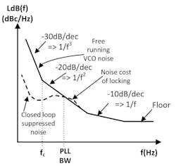
1. Here the phase noise of a free-running VCO is compared to the same VCO when phase-locked, showing the noise suppression within the loop bandwidth. In this article, the dB value of phase noise will be referred to as LdB(f) = 10log(L(f)).
In Fig. 1, the −30 dB/decade part of the free-running slope below frequency fc is flicker noise dominated, which is predominantly caused by baseband flicker noise in the amplifier mixing up around the carrier. The −20 dB/decade slope is a basic indicator of Q in the oscillator loop. The −10 dB/decade part of the slope is typically only be seen in very high Q oscillators. The floor is generated by the thermal noise raised by the gain and noise figure of the active device.
In the locked state, the phase noise above the loop bandwidth converges toward the free-running noise. Below the loop bandwidth, the noise is suppressed by feedback that strives to keep the phase noise equal to the multiplied phase noise of the reference source, which is usually lower than free-running as the reference is a very-high-Q crystal oscillator.
The phase noise as shown in Fig. 1 is single-sided. Consideration of total noise on both sides, the “spectral density of phase fluctuation” needed to convert phase noise to timing jitter, is discussed in the long version. This distinction will also be important when modeling PLL phase noise in SPICE, a subject presented in the long version of Part 3.
Induced Noise in the VCO
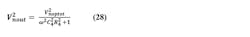
Basic Induced Noise: Noise on the input (steering) voltage of the VCO will induce a sideband to carrier spectral component according to:
We shall refer to this important relationship as the “VCO Noise Modulation Function.” This equation is derived by small signal FM theory; a form of it is given in most introductory communications theory text books. Here KHz is the same Hz/V steering function of the VCO used in Part 1. In the derivation Vn is the rms value of a sinusoidal term. However, if Vn is a spectral-noise density, then this sideband to carrier becomes a phase-noise density. Since this expression was derived using voltage ratios, converting it to phase noise in dBc is done using 20log.
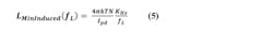
In synthesizer design this expression is of critical importance because the loop and loop filter do place noise at the VCO steering input that’s translated to phase noise output. Naturally, it’s desired for this induced phase noise to be below the free-running noise of the VCO that is approximated by Leeson’s equation (see below).
The noise modulation function may also be used to find the phase-noise term due to noise on the supply. The VCO frequency is typically a secondary but important function of supply voltage with a “steering” gain KpHz that’s generally about one order of magnitude less than KHz. Noise is modulated from this source to phase noise by:

We see that for both input and power-supply noise, a frequency flat noise spectral density will cause phase noise to decline at 20 dB/decade as frequency increases. Over this range of frequency, a constant (over frequency) allowed noise density on steering and power nodes may be specified that keeps induced noise below the VCO free-running phase noise on the most important 20 dB/decade part of the phase-noise curve. The VCO input noise Vn1 will include PLL loop filter noise.
With switching regulators, the suppression required to reduce the power-supply noise Vnp to negligible can exceed 100 dB. Such high noise suppression will generally require at least one active linear regulator stage plus passive filtering, and may require two active stages. The low noise required of supplies in low-noise synthesizers is an often overlooked factor (Part 4).
Loop BW and VCO KHz Effects on Phase Noise
The physical existence of the induced noise leads us to beware of noise on the VCO input and supply, and to look for effects such noise causes as a function of design choices like loop BW and VCO gain. Well inside the loop bandwidth, such noises are suppressed by PLL closed-loop action (covered in Part 3). However, at the loop BW and for as much as a decade past it (before higher filter poles take effect), we will have such noise sources inducing extra VCO noise. If this noise is approaching or above the VCO free-running noise, then it’s only when the first pole takes effect and has had enough frequency skirt to filter down such noise to be negligible that the closed-loop noise will match the VCO free-running noise.
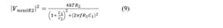
We know the minimum noise that will drive the VCO input will be given by the thermal noise of the zero resistor R2. From Part 1 we have this approximation for R2:
For the resistor thermal noise voltage, we have the standard equation (Ref. 3, pp. 8-10):
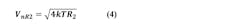
In the above, k is Boltzmann’s constant (1.38E-23) and T is absolute temperature (290 at room temp). Putting these two equations together with the induced noise relation Equation 1, we find the minimum induced phase noise at the loop bandwidth fL to be:
In the locked loop, the noise at the loop bandwidth is a critical figure of merit, and with a low-noise VCO, the induced noise of R2 is usually an important component of that noise. This induced noise represents a minimum possible noise—even if there were no other PLL noise sources and the VCO were noise-free, this noise would still exist as the cost of locking the VCO.
Additionally, this equation shows that for any given fL, this important noise component at this critical loop bandwidth frequency is proportional to KHz. It explains why higher voltage VCOs with lower KHz are theoretically capable of lower noise, and despite recent advances in integrated performance remain an optimum solution in some applications.
Leeson’s Equation for VCO Noise, and its Consequences
The Expanded Leeson Equation
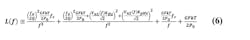
A detailed expression for VCO phase noise is given below, which is an expansion of the famous equation first developed by Leeson (Refs. 2 and 5) and further developed by numerous authors. This expression is a linear power ratio, so to convert it to dB, we use 10log. The equation is good to about +/-2 dB. We will use the variable “L(f)” for linear carrier-to-noise power ratio at offset “f,” and “LdB(f)” for the decibel variant. In this expression, f is offset frequency, fo is carrier frequency, fc is the flicker noise corner, k is Boltzmann's constant, Q is loaded resonator Q, G is loop gain in compression (the reciprocal of VCO loop loss given by 1 – QL/Q0), F is noise factor in compression, KHz is VCO gain in Hz/V, KpHz is VCO power supply pulling in Hz/V, Vn1 is spectral noise density at f on the steering input, Vn2 (also called Vnp at other points in this article) is spectral noise density at f on the power supply, and P0 is the power dissipated within the loop (losses from all sources). More detailed information is provided in the full version at www.longwingtech.com.
Referring VCO Noise to Input
The Leeson equation and the earlier relationship on induced noise show that VCO noise at any frequency can be referred to the VCO input as a noise voltage that generates that same VCO noise on the output of a noiseless VCO. Given L(f) or LdB(f) we may write for input referred VCO noise Vnvco:

It was discussed earlier that noise on the power supply also generates noise on VCO output, which will often require ultra-low-noise supplies for the VCO (to be discussed in Part 4). It will be useful in calculations and modeling to also refer the sideband-to-carrier effect of noise on the supply to the VCO input, where it can be rms summed with the other noises on that critical node, and then processed by the loop. Supply noise density is referred to the VCO input according to:
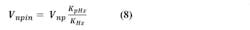
In this equation, KpHz is the VCO gain with respect to the power-supply input in Hz/V, Vnp is the spectral voltage noise density of the supply, and Vnpin is the supply noise referred to the steering input of the VCO.
Advantage of Higher Frequency
Detailed examination of the terms of Leeson's equation above will show that if Q can be maintained, the phase noise typically goes up approximately 3 dB for every doubling of the frequency. However, phase noise is reduced 6 dB by every divide-by-2, so using a higher frequency VCO can reduce free running phase noise by about 3 dB for each double and divide. These divides are often conveniently available in programmable form on modern synthesizer chips. Furthermore, this reduction using higher VCO frequency and dividing down is not just the VCO, but the in-band noise of the synthesizer as well. These are among the primary reasons for the success of the integrated VCO synthesizer.
High-Voltage, Low-KHz VCO Noise Improvement
When better far out noise is needed than a fully integrated VCO synthesizer can provide (discussed in Part 5), the usual method is a discrete higher voltage VCO with low KHz. A discrete VCO allows for higher Q than integrated, and Leeson’s equation shows noise is inversely proportional to Q2, so this is a very strong effect. A higher-voltage VCO allows greater voltage swings and higher power as well, and Leeson’s shows phase noise being inversely proportional to power. A third significant effect favoring the discrete higher-tune-range VCO is that covering a given tune range allows for lower KHz, and as shown above, induced phase noise power is directly proportional to KHz. These factors can enable an extremely low-noise discrete VCO to sometimes offer a superior noise solution at medium offsets, and quite often at far out offsets.
Converting Phase Noise to Time Jitter
See the full-length version of Part 2 at www.longwingtech for these relations.
Passive Part Noises
See the full-length version of Part 2 for descriptions and equations of noises other than thermal. These include excess resistor (current) noise, and the noises of ceramic, tantalum, and film capacitors.
Filter Noises and Limits
Noise in the loop filter is usually strongly suppressed well inside the loop bandwidth, as will be presented in Part 3 and demonstrated in the examples of Part 5. But, around the loop bandwidth and for up to a decade or so past the loop bandwidth, the filter’s noise may dominate the phase noise.
It was shown earlier how the minimum induced noise is given by R2 thermal noise, and that this noise power is proportional to the product of loop bandwidth fL and VCO gain KHz. As loop bandwidth is directly proportional to R2, and other resistors in the passive loop filter generally scale with R2, the filter noise may set limits on the bandwidth to be used in the PLL. The active loop filter has the advantage that the largest resistor noise will generally be from R2, but the disadvantage of op-amp and reference noises. In the active filter case, the noise current of the op amp also flows through R2, and this can be an even worse noise source than the thermal noise of R2.
Second-Order Passive Filter Noise
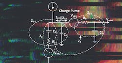
The 2nd order passive filter has the form shown in Figure 2.
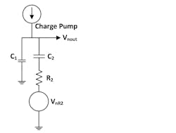
2. Shown is the second-order loop filter with its single noise source, the thermal noise in R2.
Analysis of Fig. 2 yields:
If the noise of the charge pump and dividers is modeled as a noise current Ipn, then:
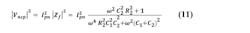
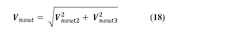
The total filter noise voltage squared is then the sum of these two noise powers. This form of loop filter is the lowest possible noise, as it only has R2 as an internal noise source. This equation may be reused for the R2 noise term in the slow slew active loop filter also.
Third-Order Passive Filter Noise
The third-order passive loop filter is shown in Figure 3. In analyzing for Vnout, we define several intermediate impedances. For example, Z3-1 is the impedance of C1 in parallel with the series impedance of R3 and C3. Z2-1 is the impedance of C1 in parallel with the series impedance of R2 and C2. We then apply voltage and current division to the different blocks.
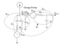
3. Depicted here is the third-order passive loop filter with intermediate impedances defined for finding Vnout, and its two thermal noise sources.
Going through this process, we find the below set of equations.
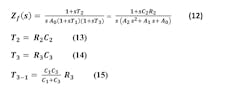
The noise from R2 at the output is:
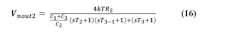
The noise from R3 at the output is:
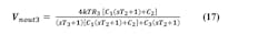
And then finally,
Both R2 and thus R3 are smaller with the lower N value of modern fractional N synthesizers with high phase-detector frequencies (see second-order normalized form approximation of R2), as compared to older integer N designs, and thus have lower noise.
Oftentimes, R3 is in the range of about R2 to 3X R2. We may thus approximate the noise voltage to expect from the properly designed third-order passive loop filter to be about 1.5 to 2X that of the second-order filter. This lower R2 and R3 value, along with higher frequency to be divided down to the application frequency, and the higher phase-detector frequency and loop bandwidth of the modern sigma-delta PLL (to be presented in Part 3), are all essential factors in lower total noise.
Third-Order Buffered Semi-Active Filter
A common active filter strategy is to break the third- or fourth-order passive filter up with an op-amp buffer in the middle that drives the final one or two RC stages, which shall be referred to here as “semi-active.” This can be beneficial if the noise of R3 and R4 is noticeable (since smaller resistor values may be used in the active case), if moderately greater tune voltage is needed, or if VCO input leakage current is on the high side of typical. Since it’s not the most recommended active filter form, its analysis and design is deferred to the full version of this article posted on the Longwing website.
Fourth-Order Active Filter Noise
The design methodology for the “slow slew mode” fourth-order active filter was given in Part 1 of this series (Fig. 4). This active filter architecture is designed to reduce the bandwidth and slew-rate requirements on the op amp, at which it’s partially successful. The use of the inverting mode with R2 and C2 in the feedback path allows this form to provide higher tune voltages with low noise gain. Current flows through R3 and then through R2-C2 to charge up the op-amp output to whatever voltage is needed. The input RC is intended to shield the op amp from the high slew rate and bandwidth of the charge-pump output.
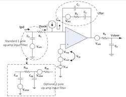
4. The fourth-order active loop filter with the option to become fifth order. The noise sources to be analyzed are shown.
However, despite its benefits in limiting the op amp’s exposure to high-frequency signals from the charge pump, it may be advantageous to add an additional input RC stage. As pointed out by Banerjee, experimental evidence (Ref. 4, 5th ed., pp.371-372) indicates that the op amp in an active loop filter not being fast enough sometimes seems to cause a several dB rise in the 1/f noise of the PLL. This is presumably due to pulse widening, which allows through more charge-pump 1/f noise.
The noise on steering output of the active filter may be characterized as the sum of the noise powers from the plus input, from the minus input, from the forward impedance, and in the final RC stage.
The minus input internal filter noise is the thermal noise of R3, gained up by:
We can generate this noise over frequency using the next several relationships.

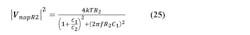
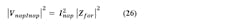
Next, we consider the gained noise from the plus input of the op amp. This is the rms sum Vnp of the reference noise and the op amp’s own noise, appropriately gained, given by:
The magnitude squared functions below are convenient to use.
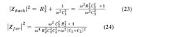
The noise generated by R2 is found by taking into account that the minus input of the op amp is a “virtual ground.” Op-amp feedback holds it equal to the plus input, so noise from R2 comes straight through to the output, except for being filtered within Zfor when C1 > 0.
The noise generated on the op-amp output by the op-amp noise current is again found by noting that the minus input is kept equal to the plus input by op-amp feedback. The only way for that to hold is for Inop to flow totally through Zfor and not through Zback.
For the sake of convenience, we may count the noise of R4 as part of op-amp output. We now have all the noise terms at the op-amp output.
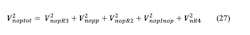
This noise needs merely to be passed through a now noiseless R4-C4 filter to give the noise from the active filter to be presented to the steering input of the VCO.
With the above, we have all of the major open-loop noises to be shaped by the loop except for what is sometimes called the “PLL noise.” This is something of a misleading term, since it typically means just the noise of the charge pump and dividers in the synthesizer IC, not the total PLL noise. It’s not given above in the noise sources review, as it’s normally specified as a closed-loop noise after shaping. It will be covered in the next article along with the methods for analyzing how noise is shaped, optimum loop bandwidth, and the synthesizer IC figure of merit for evaluating chip noise.
Series: Ultra-Low-Noise Synthesizer Design
Farron Dacus is an RF design consultant in Dallas, Texas. He received his BSEE and MSEE from the University of Texas, and has over 30 years of experience ranging from ICs to circuits to systems in low-noise RF, short-range radio / IoT, cellular, military communications, and aircraft radios. He may be reached at [email protected].
References
1. “Design Methods of Modern Ultra-Low Noise Synthesizers,” Microwaves & RF, Farron Dacus, Dec. 2018.
2. Microwave and Wireless Synthesizers, Theory and Design, Ulrich L. Rohde, John Wiley and Sons, 1997.
3. Low Noise Electronic System Design, C.D. Motchenbacher and J.A. Connelly, John Wiley, 1993. This outstanding classic work is highly recommended.
4. PLL Performance, Simulation, and Design, Dean Banerjee, first edition 1998. The 5th edition of this outstanding reference, published in 2017, may be freely downloaded at: http://www.ti.com/tool/pll_book
5. Fundamentals of RF Circuit Design with Low Noise Oscillators, Jeremy Everard, John Wiley and Sons, 2001. This reference is particularly excellent for its detailed examination of Leeson’s Equation, with variations for how impedance is defined and used within the oscillator loop.

About the Author
Farron Dacus
RF Design Consultant
Farron Dacus is an RF design consultant in Dallas, Texas. He earned a BSEE and MSEE from the University of Texas. Farron has over 30 years of experience ranging from ICs to circuits to systems in low-noise RF, short-range radio/IoT, cellular, military communications, and aircraft radios.
