Noise and its Shaping in Ultra-Low-Noise Synthesizer Design
Series: Ultra-Low-Noise Synthesizer Design
Download this article in PDF format.
This third part in our low-noise synthesizer design series is the medium-length online version. In print are the abridged versions, while full-length versions are available at www.longwingtech.com. Part 1 (Dec. 2018) covered basic design for functionality and stability. Part 2 (Feb. 2019) covered the many noise sources in the synthesizer outside of the actual synthesizer IC. This third article looks into synthesizer IC noise, the closed-loop shaping of noises, and related issues such as optimum bandwidth.
Here, a key metric for characterizing synthesizer IC noise is developed. This material also leads directly to analysis of optimum loop bandwidth, taking all noise sources into account—a key design topic that to the author’s knowledge is not published elsewhere. For reasons of space, some important parts of this subject are deferred to the full version on the Longwing website. The long-version material includes derivation of charge-pump noise in current form, spur noise, SPICE modeling of PLL noise, and application noise requirements. Part 4 will review parts and tools available to the low-noise synthesizer designer. The concluding Part 5 will present low-noise design examples.
Recent years have seen major changes in the frequency synthesis art. Ultra-low-noise discrete VCOs, which still enjoy a 20- to 30-dB phase-noise superiority over the best integrated VCOs, are no longer always the preferred solution. Integrated VCOs are now paired with sigma-delta fractional-N architectural innovations, often allowing them to have not only surprisingly good noise performance, but often superior performance, particularly for applications where closer in phase noise is the issue.
The ways to achieve such performance may be understood from the noise-shaping material in this article. The ultra-low-noise discrete VCO remains superior for higher offset frequency (beyond the loop bandwidth). Part 5 will provide an example illustrating how discrete VCO design could potentially be extended to use these same methods to maintain superior performance at lower offsets. It remains to be seen whether such designs allowing discrete VCOs to recapture their originally superior noise performance in the locked state will emerge.
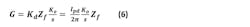
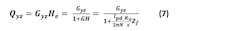
Noise Transfer Functions and Total Synthesizer Noise
Part 2 gave the main open-loop noise sources in the PLL. Now, we turn our attention to how these noises are shaped by the PLL into the closed-loop noise. A fundamental feature of the modern, high bandwidth PLL is that the very low noise of the input crystal reference is transferred to the VCO, for frequencies within the loop bandwidth, down to the noise floor allowed by the synthesizer IC’s own noise (dividers and charge pump). Beyond the loop bandwidth, the VCO reverts to its own free-running noise, hopefully only slightly degraded by filter and power-supply noise.
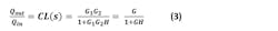
In Part 1 of this series, particularly the online and full versions, the transfer functions pertinent to finding part values for loop bandwidth and phase margin were introduced. We now go further with this approach, considering the noise transfer functions within the loop. It is helpful to first present this in a generalized form, using the feedback tracking loop of Figure 1.
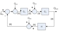
1. A generalized feedback tracking loop with noise “Q” injected at various spots is useful for deriving the noise transfer functions from a point “y” to a point “z.” Here, the forward gain G is broken up into G1 and G2 for generality.
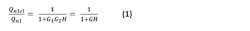
Example noises can be injected at various points labeled (1) to (6); we are interested in deriving the closed-loop resulting noise at any point in the loop. If we inject open-loop noise Qn1 into point (1), we will get a closed-loop quantity Qn1cl on point (1) after the loop acts on this noise. The ratio of closed loop to open loop will be given by:
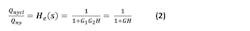
When the above block diagram represents a phase-locked loop, this function is the high-pass “error transfer function” He(s) that was given in the online and long versions of Part 1. If we check any other point in the loop, where we inject noise into a node and find the ratio of closed-loop noise on that node to the injected open-loop noise, we will get the same function except for reordering of the factors G1, G2, and H. So:
Another critical function is the “closed-loop transfer function” CL(s) as described by Banerjee:
The classic “phase transfer function” is given by:
In older books, Hclassis is called simply H, whereas in more modern books, H is used for the feedback block and H = 1/N. The term Hclassic is used here to try to avoid confusion.
Note that CL(s) and Hclassic(s) look like scaled versions of He, but this scaling by G or GH is not flat with frequency. Because forward gain G has two integrators in a PLL (the loop filter and the VCO), the net result is that G>>1 within the loop bandwidth, and CL(s) and Hclassic are converted to low-pass form. Figures demonstrating this are shown in the full version of this article.
If we examine the noise from any point “y” into which we inject noise Qny into the loop, to an output node “z,” where Gyz is the gain from point y to point z, we find the convenient relation:
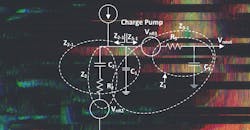
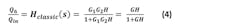
With this generalized information in mind, we may now consider the PLL block diagram of Figure 2.
2. General PLL block diagram with noise sources. Note the phase noise equations contained in the figure for converting rms summed voltage noise Vnsteer to phase noise, which were derived earlier. Many noise sources use a math processing program like Mathcad or MatLab, which is recommended for calculations and graphs of noise terms and total noise. SPICE may also be used to build a behavioral model of the loop that provides noise.
The noise sources of this figure are:
Vnx: The steering input-referred noise of the crystal reference oscillator, from its datasheet and then modified by the VCO noise modulation function to refer to input.
Vnxsteer: The noise of the crystal steering input; for example, filtered DAC noise used to trim the crystal frequency.
Vnxpwr: The input-referred noise from the crystal-oscillator power supply, as described in Part 2.
Kx: Steering gain of the crystal reference in rad/sec/V. When referring noise to the crystal-oscillator input, Kx should be converted to KxHz.
Inpll: The noise of synthesizer chip dividers and charge pump represented as a noise current, as derived in the full version.
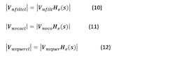
Vnfilt: The output filter voltage noise density presented to the VCO steering input.
Vnvco: The Leeson noise of the VCO referred to its steering input.
Vnvpwr: The noise effect of VCO power-supply noise referred to the VCO input.
Graphs of the phase and error transfer functions are shown in the full-length version. To make use of the transfer function relationships derived above for the particular PLL case, we will need detailed filter functions. These are given in Table 1 of the full version on the Longwing website. With a particular filter designed and with noise sources identified, we have what we need to find the closed-loop noise. For the PLL block diagram with noise sources as given, we may write:
The voltage noise or noise sideband to carrier (depending on whether the output node variable is in volts or in rad/sec) generated by noise “x” at point “y” is given by:
Now, we may use this relationship with the input noises to generate the rms sum of closed-loop noises on the VCO input, and then the VCO noise modulation function to give the closed-loop phase noise on the output.
From the rms sum of noises on the crystal oscillator tune input (or output), we get an open-loop phase noise on the crystal output θnref. This is divided by “R” and summed into the loop at the phase detector. The closed-loop phase noise at the (imaginary) node following feedback phase summing is θnrefcl = θnref He. We use the “magnitude” function to emphasize these are rms noise quantities. Therefore, the reference noise as modeled at the VCO input will be:

The noise from the charge pump and dividers of the synthesizer chip (often called “PLL noise”) is normally handled directly at the VCO output, using methods developed by Banerjee. These methods shall be presented later, but first we will develop the method of summing all noise sources to get total phase noise.
We assume here that we have a frequency-dependent current noise function inpll that can be summed into the loop filter using the transfer function approach developed above. This noise current function is derived from the Banerjee model in the full-length version. Besides allowing a unified noise-analysis approach, this new model is convenient for SPICE simulation. The noise voltage at the VCO input from the charge pump and divider noise is:

The closed-loop noises for the loop filter, input-referred VCO noise, and input-referred VCO power supply noise are all on the VCO input, so they are simply the open-loop noises multiplied by He:
It is enlightening to graph these noises separately to identify whether it is worth more effort or parts cost to reduce total noise.
The magnitude of the total noise on the VCO steering input is given by the rms sum of the above sources:

Finally, this rms summed total noise voltage on the VCO input in the closed-loop state is transformed to a total output phase noise by:
Charge Pump and Divider Noise and Corner, Synthesizer IC Figure of Merit, and Modeling
This charge pump and divider synthesizer IC noise is often called “PLL noise.” That term is avoided here, though, because confusion could arise as to whether this is one component of many, or total PLL noise. Let’s coin the term “CPD noise” as an accurate alternative.
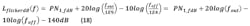
Flat Synthesizer Noise: Banerjee (Ref. 3) seems to have been the first to analyze and quantify this important noise source (Ref. 4) to useful accuracy in a way that can be specified in synthesizer datasheets. While not actually flat, inside the loop bandwidth it tends to be only a weak function of frequency. The physical source of this noise is the charge pumps and dividers. Over the years, as synthesizer ICs have become faster and pulse widths have approached zero, this noise has dropped significantly.
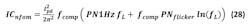
We can intuitively understand this noise as follows. For any given pulse width with a given jitter, we can hypothesize that there will be a floor to this noise, a term proportional to the comparison frequency (number of the narrow pulses per unit of time), and a multiplication term similar to that in multiplying the crystal-reference phase noise (note the jitter noise is at the phase-detector input, and adds to the jitter of the crystal reference). The resulting “flat” noise (not counting yet for a 1/f behavior to this CPD noise) is given by:

Here “PN1Hz” is the normalized floor on a per-Hz basis. It is typically given in dB, but we will have occasion to convert it to linear when adding flat and 1/f noise powers. The empirical approach supporting this equation is proven in Ref. 4, where a timing jitter analysis leads to the same results. PN1Hz is now a standard datasheet parameter.
Inside the loop bandwidth CL(f) ~ N, and:

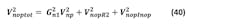
Because N = fout/fcomp, we may write:

Since there’s noise in each phase detector pulse, the reduction of 3 dB of in-band noise for each doubling of fcomp in the above relation may seem odd. Doubling fcomp adds 3 dB to the noise contributed by the phase detector pulses. But, doubling fcomp also reduces N by two, which removes 6 dB of noise multiplication. The net is the 3-dB improvement shown.
This simple equation has powerful results for the synthesizer industry. As radio designers, we are normally given fout, and by using a smaller N value, we get higher fcomp and lower in-band phase noise while generating that fout. This method is being strongly applied by semiconductor companies with modern sigma-delta fractional N synthesizers, with comparison frequencies now up to 100-200MHz (Part 4) and loop bandwidths ranging up to hundreds of kilohertz. This is key to allowing on-die VCOs to have effectively low noise at required phase-noise offsets, which despite heroic design efforts to improve their phase noise, are still significantly noisier than the best discrete VCOs (Part 4). The equation is the very heart of why fully integrated synthesizers can be sufficiently low noise for most modern applications.
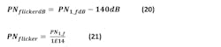
Flicker Synthesizer Noise: The method adopted by Banerjee to model 1/f noise in the synthesizer chip is to assume that flicker dominates in-band noise at 10 kHz, and to scale that noise by output frequency relative to 1 GHz and by offset relative to 10 kHz. This gives:
The term PN1_f is used by Analog Devices as a 1/f noise parameter and can be found in the company’s datasheets. Texas Instruments refers to this same term as PNPLL_1/f. These are typically provided in dB form. In the equation above, the suffix “dB” is provided to make this clear.
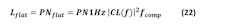
Linear Technology uses this same basic method for specification, but eliminate references to 1-GHz carrier and 10-kHZ offset. They use the normalized 1/f noise term LM(NORM-1/f). Let’s refer to this term with the simpler variable PNflicker when in linear form and PNflickerdB when in dB form. Their equation is:

Comparing these two equations, it is seen that:
Combining Flat and 1/f Synthesizer Noise: To add flat power to flicker power to get a total synthesizer chip noise power, we need linear terms, which are:
Within the loop bandwidth:

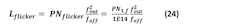
The total charge pump and divider noise at f = foff is given by:

Assuming that the flicker corner is within loop bandwidth, we may set the flicker and flat noises equal to solve for corner frequency at a particular output frequency, N, and fcomp. When we do this and substitute N = fout / fcomp, we get as a synthesizer IC in-loop bandwidth corner frequency:

There will also be a generally closer-in corner where multiplied crystal frequency will become dominant over synthesizer IC 1/f noise. Depending on the noises in question, this can range from less than 100 Hz to several kiloherz.
Current-Noise Model: The above noises are expressed on the VCO output in the closed-loop state. Synthesizer CPD noise can be expressed as a sum of a flat and 1/f noise current injected into the loop filter in parallel with a then assumed noise-free charge-pump current. This form is useful for SPICE modeling of the synthesizer noise. The analysis to determine this noise is given in the full version. The results for the combined flat and 1/f noise are:

Synthesizer IC Noise Figure of Merit: Note that a lower PN1Hz, a superior flat noise, will give a higher corner frequency for the same flicker noise profile. So, a higher corner does not necessarily denote a higher noise part. To understand when a part is actually superior, the 1/f and flat noises may be combined to give a reliable figure of merit for the total synthesizer IC noise, over a desired bandwidth fL and with a desired phase detector frequency fcomp. If the synthesizer chip noise current inplltot is integrated from 1 Hz to fL, we obtain a noise power figure of merit:
If two chips do not allow the same Ipd and fcomp to be used, then this equation with the Ipd and fcomp for each chip gives a figure of merit for noise power, where the lowest number is superior. Any time we are comparing two ICs with the same Ipd and fcomp, the figure of merit may be simplified to:

Optimum Loop Bandwidth Counting All Noise Sources
The “ideal bandwidth” generally means a bandwidth where the “flat” in-band noise (which will not be exactly flat) intersects the VCO free-running noise at the loop bandwidth. A lower bandwidth would mean that the VCO noise at the loop bandwidth is higher than the flat in-band noise floor that will be reached, which will look like significant noise peaking around the loop bandwidth. A higher bandwidth will mean that the noise induced by the synthesizer IC will be higher than the VCO free-running noise at the loop bandwidth. These effects are shown in Figure 3.
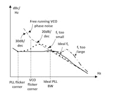
3. Illustration of ideal bandwidth versus noise effects of too small or large a bandwidth.
A possible limit to reaching ideal bandwidth is sigma-delta noise, which tends to peak around one half fcomp, and may require using a moderately lower bandwidth. However, we may use our knowledge of the noise sources to find the ideal bandwidth where the VCO plus filter noise will match the synthesizer-chip-induced noise. Because the bandwidth and noise are functions of each other, some iteration may be needed to arrive at the best possible solution.
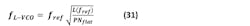
Ideal Passive BW for VCO Noise and Flat Synthesizer IC Noise Only: Ignoring any noise modulation of the VCO by the loop filter and the flicker corner of the synthesizer IC, we can easily find the approximate ideal bandwidth from setting Lflat = LVCO and solving for f. This is the approach recommended by Banerjee for minimum jitter (Ref. 3, 5th edition, pp. 305-306).
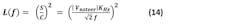
Assuming the desired fL will be on the −20 dB/dec part of the phase-noise slope, and that we know the phase noise L(fref) (converted from dB), the VCO noise at a frequency fL (the desired bandwidth) will be given by:

From this ideal bandwidth, fL-VCO, considering only VCO noise, is:
The issues we run into with this first-order approximation are that we don’t really get to perfectly maintain the free-running VCO noise due to noise modulation by filter resistors, and that the synthesizer IC flicker noise may not be negligible at the resulting bandwidth. We can usually use sufficiently low power-supply noise whereby supply noise modulation is negligible, as very-low-noise integrated regulators have become recently available; if they won’t do, then still lower noise can be provided by discrete solutions (Part 4). However, the filter noise will usually be at least noticeable and at least moderately alters the free-running VCO noise.
Ideal BW with the Passive Loop Filter Including Synthesizer and VCO Flicker Noises: We get a more accurate measure of the optimum minimum jitter bandwidth when these noise sources are taken into account. Such noise sources may lead to either an increase or decrease in ideal bandwidth to that predicted using VCO noise alone. Adding loop filter noises and VCO flicker noises will push out the ideal bandwidth. But, counting in the higher synthesizer IC noise with synthesizer flicker tends to push toward a lower intersection. In a particular case, either one of these may dominate. There are also noise terms from the crystal-reference oscillator, but these will usually be negligible until lower offsets, as they come to dominate the locked noise on the order of 50 Hz (ovenized super-low-noise reference) to about 3 kHz (mobile handset class VCTCXO). The crystal noise would tend to push to a lower locked bandwidth as ideal.
When we consider ideal bandwidth with the noise of a filter added to the VCO noise, in the frequency range where the bandwidth fL will fall on the −20 dB/dec part of the VCO phase noise, and take account of synthesizer flicker noise, we may write:

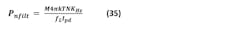
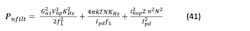
For the passive filter, the noise comes from the resistors in the filter. We are mostly interested in the noise at the loop bandwidth, where it’s neither suppressed by the loop or filtered off by higher-order poles. At this frequency, using the thermal noise and the VCO noise modulation function:

In this equation for Pnfilt, “M” is a multiplier for filter form. M = 1 for the first- and second-order filter (only R2); M is generally about 2-3 for the third-order form (adding R3); and M is generally about 3-4 for the fourth-order form (adding R3 and R4). Now, we can get a good approximation for R2 from the second-order PLL equations, where:
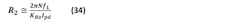
Substituting this into the equation for passive filter noise:
We may substitute this relation for Pnfilt and the linear expressions for Pnvco and PNflat into Equation 32, and solve for ideal bandwidth fL. Because the expression for Pnvco as a function of frequency is second order, the expression for Pnfilt is first order, and the expression for Pnflat is constant, we end up with a quadratic equation:
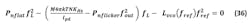
In this quadratic equation, fref is not the phase detector frequency fcomp, but the point on the −20 dB/dec part of the VCO slope where we get an example measure of VCO phase noise. Here, 10 kHz is most commonly used, but if the VCO flicker corner is not well below 10 kHz, then a higher reference frequency should be chosen. Now, solving for ideal fL, we of course get:
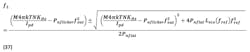
This solution will always have a positive and negative frequency result, so there’s never any doubt as to the correct root.
Note in the above that it was assumed that the final bandwidth was at a frequency greater than the VCO flicker corner. This is often—but not always—true. If the final bandwidth calculated using the above is in fact below the VCO flicker corner, then we must modify our design procedure. This is done by noting that for frequency fL below the flicker corner fcvco of the VCO, we have a more complicated equation for VCO free-running phase noise:

Now when this relation for VCO phase noise is used to find fL, we get a cubic relationship that needs to be solved numerically:
Ideal Bandwidth for the Slow Slew Active Loop Filter: This inverting form loop filter is the most recommended for those cases where the better medium and far out noise of a low-noise, high-tune-range discrete VCO is worth the extra cost and board area. An expression for the noise terms in the output of this filter was derived in Part 2 (Ref. 2).
Since we’re concerned with the noise at the loop bandwidth when deriving ideal bandwidth, we can leave off the term for the noise of R3. This noise is negligible at the loop bandwidth because the input pole is well above the bandwidth, the backward impedance is much greater than the forward impedance, and thus the noise gain relative to this term is <<1. Similarly, R4 can be of such low value relative to R2 that we can neglect its noise as well for the purpose of finding bandwidth. We will also assume that VCO supply noise has been made low enough to be negligible (see Part 4). Thus, the filter noises we use are:
Recall in the above that Vnp is the combined op amp and reference noise. Gn1 is the noise gain for the op amp plus input, which will usually be a small number in the range of about 1.005 to 1.02. It will be nailed down once the loop bandwidth and loop filter are fully defined. Next, we translate this noise to VCO output using the VCO noise modulation function, which gives:
We recall the VCO noise including noise below its flicker corner as:

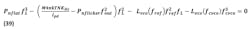
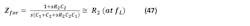
The main equation to use if setting VCO and filter noise equal to synthesizer IC noise at the loop bandwidth fL is:

The above equations may be combined to give this equation cubic in fL:
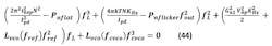
Here, the noise gain Gn1 from op amp plus input to op amp output at the loop bandwidth is given by:
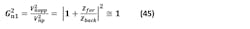
The expressions for Zfor and Zback developed in the full-length version of Part 2 may be approximated at fL as:
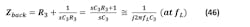
To the author’s knowledge, the above cubic relationship for fL is the most accurate published relationship for getting an initial value for ideal loop bandwidth, as it takes all of the major factors into account. However, it still relies on several approximations, which are discussed in the full-length version along with more detailed analysis recommendations.
If we ignore the VCO flicker corner on the assumption the loop bandwidth exceeds the VCO corner, then the cubic equation reduces to:
Ideal Bandwidth for the Semi-Active Buffered Loop Filter: The ideal bandwidth for this filter form is analyzed in the full-length version, available on the publications page at www.longwingtech.com.
SPICE Modeling of Synthesizers and Their Noise
SPICE and similar CAD modeling is, of course, one of the greatest advances in electronic design history, allowing for excellent results when component models are accurate. The mathematical analysis is more flexible than SPICE, but it’s quite a chore to juggle all of the noise sources and control system behaviors described above. Handling this mass of data can easily lead to making mistakes.
A SPICE analysis can confirm the correctness of the mathematical analysis, and often be more accurate. Doing both for cross-checking and then having each analysis form available to take advantage of their particular strengths gives designers the best of both worlds. Methods for using SPICE in PLL noise analysis are provided in the full version.
Spur Noise
Spurs are discrete frequency components most commonly caused by digital noise on the phase detector output; they get through the loop filter in at least noticeable form and cause modulation on the input of the VCO. These “modulated” spurs are thus symmetrical about the carrier. “Direct” spurs also exist. For instance, reference or clock noises that leak around the loop filter are present in ground plane noise, or come in through the power supply. These are discussed in the full version, and in greater detail in the references given there.
System Phase-Noise Requirements
This article series will not take the space to derive system requirements of multiple systems in high detail. However, as such requirements are seldom given in synthesizer text books, some approximate example requirements are derived in the full-length version.
Summary
In recent years, synthesizer IC noise has been drastically reduced, and, in turn, the architectural advances of high-bandwidth sigma-delta synthesizers has allowed outstanding in-band noise suppression. Lower noise and higher-frequency references that further support low in-band noise are also becoming available at outstanding cost reductions compared to the price of low-noise ovenized references. In this situation, even the noise of on-die VCOs can be suppressed to the point of allowing fully integrated synthesizers to address most applications, at least for lower offset frequencies. Discrete VCOs still retain their classic noise advantages at higher offsets, and in some cases remain the optimum solution.
Key parts and their noise behaviors will be reviewed in Part 4. The examples in Part 5 will explore how the advantages of discrete VCOs could be combined with the latest sigma-delta synthesizer technology to allow discrete VCOs to regain their historical advantages. This would require that discrete VCOs be extended to higher frequencies while retaining their higher Q and higher tune range advantages over integrated VCOs. It remains to be seen if this situation will develop.
Series: Ultra-Low-Noise Synthesizer Design
Farron Dacus is an RF design consultant in Dallas, Texas. He holds a BSEE and MSEE from the University of Texas, and has over 30 years of experience ranging from ICs to circuits to systems in low-noise RF, short-range radio / IoT, cellular, military communications, aircraft radios, and short-range Doppler radar systems. He may be reached at [email protected].
References
1. “Design Methods of Modern Ultra-Low Noise Synthesizers,” Microwaves & RF, Farron Dacus, Dec. 2018.
2. “Noise Sources in Ultra-Low Noise Synthesizer Design,” Microwaves & RF, Farron Dacus, Feb. 2019.
3. PLL Performance, Simulation, and Design, Dean Banerjee, first edition 1998. The 5th edition of 2017 of this outstanding reference may be freely downloaded at: http://www.ti.com/tool/pll_book.
4. Applied Radio Labs, application note DN006.

About the Author
Farron Dacus
RF Design Consultant
Farron Dacus is an RF design consultant in Dallas, Texas. He earned a BSEE and MSEE from the University of Texas. Farron has over 30 years of experience ranging from ICs to circuits to systems in low-noise RF, short-range radio/IoT, cellular, military communications, and aircraft radios.
