Testing Interconnect Designs for 5G, 6G, and Phased-Array Systems
What you’ll learn:
- What is a PCB launch and why is it so important?
- The impact of phase stability on phased-array designs.
- How return loss and insertion loss are impacted by test fixture design choices.
6G systems will be able to operate in a wide range of frequency bands, including current 5G frequencies in the sub-1-GHz range, the 3.5- to 6-GHz mid-band and mmWave range, and new frequencies in the 7- to 15-GHz centimetric range and 90- to 300-GHz sub-terahertz range. We can expect lower frequency bands to remain extremely important as essential spectrum for coverage, capacity, and mobility in the 6G era.1
Test fixtures to support these frequencies must be carefully designed to simulate the real-world performance of RF and microwave systems, such as those used in 5G, 6G, phased arrays, and other applications. This article describes methods to create an optimal test setup for a PCB signal launch/interconnect design, including de-embedding techniques and calibration using measured data.
Technical Challenges in Designing Interconnect Systems
For 5G/6G and phased-array applications, the interconnect system design needs to support high density (with more physical channels in a reduced space), high linearity (with no suckouts or nonlinear phase changes in the band), and repeatability after mating/unmating the interconnects (especially in initial system bring up).
Our work has revealed two key areas that designers can focus on to achieve the necessary performance of the test fixture and, ultimately, the interconnects. The first is to avoid connector misalignment, and the second is optimizing the signal launch on the PCB (which requires a test setup to achieve accurate device-under-test, DUT, measurements).
It was also discovered that, for high-density routing, implementing every layer interconnect (ELIC) technology on an HDI PCB substrate can help move the frequency at which higher-order modes propagate to well above the bandwidth of interest. In addition, using high-density, compression-mount ganged cable assemblies can minimize insertion loss and return loss.
Connector Misalignment: Critical but Easily Addressed
Interconnects are needed at all signal inputs and outputs. It’s known that at higher frequencies, even slight misalignments of a connector are sufficient to cause failure.2
>>Download the PDF of this article, and check out the TechXchange for similar articles and videos

PCB Signal-Launch Design Should Help Push Frequencies
The PCB signal launch is the mating structure that couples the electromagnetic energy in the connector to the PCB. This area isn’t simply the footprint of the connector, so it may be challenging to characterize. The amount of energy transferred from the connector to the PCB trace can be improved by considering connector design, PCB material characteristics and thickness, various signal launch configurations, and operating frequency.3
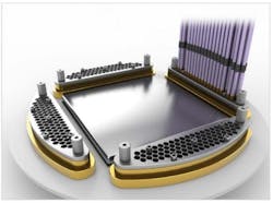
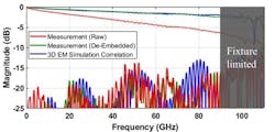
An optimized RF launch structure makes it possible to push the frequency even higher, which is beneficial because the DUT can be tested in a cleaner manner at higher frequencies (Fig. 1). Our work focused on a methodology for examining the true performance of the device under test, de-embedding the effects of the coax connector.
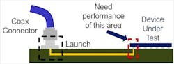
Ideally, we would connect the test instrumentation directly to the solder balls of the device, but this is impractical. Instead, the test cable, the connector on the PCB, and the trace to the DUT are de-embedded from the measurement. This process mathematically removes the test fixturing and renders it electrically invisible when looking at the device’s performance. The goal is to obtain the widest possible fixture/critical-path bandwidth.
Achieving Accurate DUT Measurements
There are very few cases where the entire fixture up to the DUT interface can be calibrated out using mechanical or electronic calibration kits. In most cases, some combination of cables, connector launches, traces, and vias need to be de-embedded from the measurement.4
Much work has been done on de-embedding algorithms used to remove fixturing contributions from measurements.5-8 All algorithms perform better when fixture insertion loss (IL) is lower and there’s greater separation between IL and return loss (RL).9
Design Principles for Reducing Insertion and Return Losses
Based on the above review, our goal was to achieve the lowest IL and RL possible for our test fixture over the frequency range of interest.
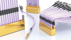
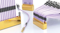
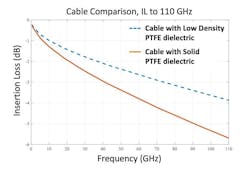
IL is directly correlated to the length of the fixture that needs to be de-embedded. Our work showed that ganged cable connectors minimize fixture IL. Figure 2 shows the comparison of PCB trace loss to two ganged cable connectors—one is a Samtec BE90A ganged connector using 0.047-in.-diameter low-loss cables and the other a Samtec BE70A using 0.086-in.-diameter low-loss cables.
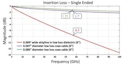
Our conclusion is that ganged cable connectors perform better because cable losses are always lower than PCB losses (making it preferable to cover more distance with cable). Further, ganged connectors have increased density, enabling lower losses by placing them closer to the DUT (Fig. 3).
For Phased Arrays, Phase Stability is Crucial
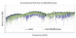
When considering phased-array systems, phase stability is a key consideration to ensure optimal performance. For consistent phase response, our work indicates that switching to a high-performance, low-loss microwave cable works very well in dynamic applications.
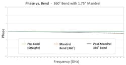
Figure 4 represents cable return loss before and after flexure out to 50 GHz. In this case, the cable used incorporates an interlayer within its construction, which we believe contributes to overall performance stability. Figure 5 uses the same cable but with a smaller diameter (0.078 in. outer diameter) for testing out to 70 GHz. The test shows little phase change even after a 360-degree bend around a 1.75-in. mandrel.
RL is heavily impacted by the performance of transitions, such as the connector-to-PCB and DUT-to-PCB. Much work was done in this area,4 with the major conclusions being that it’s beneficial to reduce the diameter of the via structures and to consider using an ELIC technology,10-11 which allows for microvias and very high-density routing (Fig. 6).
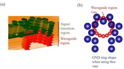
An ELIC approach can increase the cutoff frequency of the circular waveguide formed under a via transition, allowing it to be tuned independently of the GND ring in the launch area. Because ELIC only has to penetrate one dielectric layer, it’s possible to use smaller drill and pad sizes, enabling them to be more compact than through vias.
Measurement Correlation
Here we present the results for a test fixture and PCB launch designed using the aforementioned design principles (Fig. 7). Measurements were performed on a Keysight N5227B VNA with 110-GHz extension heads. The VNA was short-open-load-through (SOLT) calibrated using a Keysight 85059B calibration kit.
The goal was to measure the performance of ganged, vertical-launch cable (VLC) assemblies with rated performance up to 90 GHz. We used three inches of 0.047-in. coax and 1-mm connectors at the end of the cable.
We performed measurements by connecting the VNA to the cable side of the DUT on port 1 and a ganged VLC mounted on the PCB on port 2. There’s approximately 25 mm of trace between the ganged VLC on the PCB and the DUT-PCB interface. The ganged VLC on the PCB and PCB trace needed to be de-embedded from the measurements to isolate the performance of the DUT.
Our conclusion is that de-embedding works well to 90 GHz and DUT performance correlates very well to simulation up to that frequency (Fig. 7, again). The fixture performs to the highest bandwidth because:
- ELIC allows for the use of smaller-diameter vias, reducing the cross-sectional size of the launch and preventing excitation of higher-order modes up to 90 GHz.
- ELIC enables the circular waveguide below the launch to be completely sealed and in cutoff, again to 90 GHz.
- Even though narrow vias require the use of thin dielectrics, stacking the dielectrics allows for wide lines and low attenuation loss.
Conclusions and Future Work
Differences exist between simulation and measurement above 90 GHz, but that will need a higher-performance test fixture to resolve what is a simulation model inaccuracy versus a test fixture limitation. Ultimately, all fixtures that need to cover extremely wide bandwidths (especially down to DC) are going to experience issues related to coax size and limited very wide bandwidth discontinuity compensation strategies.
Above 110 to 120 GHz, waveguides may provide the best performance. The biggest drawback to waveguides is inflexibility and ease of connections. Therefore, flexible micro-waveguide technology could be a solution.
Using proper design considerations, flexible micro-waveguide technology can demonstrate excellent dynamic stability with negligible change in performance compared to rigid waveguides. This approach would offer flexibility and ease of use at a reduced size, thereby supporting sub-terahertz range frequencies.
Alternatively, work is being done to address bandwidth expansion of 1-mm connectors beyond their traditional 110-GHz rated frequency in support of emerging D-band applications. While 1-mm connectors for D-band aren’t fully mature, using such connectors could bridge the gap of familiar technology for test (with threaded coupling) versus using a novel interconnect solution to support the wide range of frequency bands required for 6G systems.
Because loss performance of a test fixture can be optimized when using a cable (instead of running the signal through a PCB trace, as noted previously), combining next-generation 1-mm connectors with a highly stable, high-performance microwave cable assembly could further improve loss performance, especially in dynamic applications (Fig. 8).
In summary, this article describes methods to create an optimal test setup for a PCB signal launch/interconnect design, including de-embedding techniques and calibration using measured data. Methods such as these, combined with new technologies in cables and connectors, will be critical to the success of future 5G, 6G, and phased-array systems.
References
1. Ericsson, “Sub-Terahertz Communication in 6G.”
2. M. Griesi, Z. Speraw, E. Loy, and S. Wronowski. “Millimeter Wave Design: Optimizing Performance in RF Compression Mount Connectors.”
3. Z. Speraw. “Improve Alignment of Compression-Mount Connectors in Wireless Designs,” Microwaves & RF, March 2024.
4. Signal Integrity Journal, “Signal Launch Methods for RF/Microwave PCBs.”
5. DesignCon 2024, “Realistic Use Cases of Edge, Angled and Vertical Launch Connectors Up to 100 GHz.”
6. E. Bogatin and M. Resso, “A simple, yet powerful method to characterize differential interconnects,” DesignCon 2011 Education forum.
7. X. Ye, J. Fan and J. Drewniak, "New De-embedding Techniques for PCB Transmission-Line Characterization", DesignCon 2015.
8. In-Situ De-embedding (ISD) by AtaiTec Corporation.
9. S. -J. Moon, X. Ye, and R. Smith, "Comparison of TRL calibration vs. 2x thru de-embedding methods," 2015 IEEE Symposium on Electromagnetic Compatibility and Signal Integrity, Santa Clara, CA, USA, 2015, pp. 176-180, doi: 10.1109/EMCSI.2015.7107681.
10. Multek, Every Layer Interconnect.
11. ACDi, “A Peek at the History of PCBs.”
>>Download the PDF of this article, and check out the TechXchange for similar articles and videos
About the Author
Sandeep Sankararaman
Principal Engineer, Samtec
Sandeep Sankararaman, Principal Engineer at Sametc, has 20+ years of experience in signal and power integrity for IC packages, PCBs, PCB connectors, and connectors for cable assemblies.
Shawn Tucker
Principal Signal Integrity Engineer, Samtec
Shawn Tucker, Principal Signal Integrity Engineer at Samtec, has 25 years of experience in high-performance system design, printed-circuit-board (PCB) development, interconnect modeling and measurement, and test instrumentation design. His current work focuses on RF compression-mount applications, where he brings deep expertise in advanced signal integrity and hardware design technologies.
Jim Alexander
Manager, RF Applications Engineering, Samtec
Jim Alexander is Manager, RF Applications Engineering at Samtec. Working with Samtec since 2020, Jim has spent 25 years focused on assisting customers with microwave cables and connectors. He has been involved with many projects and challenging requirements supporting programs for manned aircraft, UAVs, satellites, and radar systems. Jim has a BS in Electrical Engineering from the University of Delaware.
