Advanced Load Test Solutions Address Next-Gen Product Development
What you’ll learn:
- The challenges in advanced electronic testing.
- How power emulators tackle validation issues.
The embedded electronic landscape is evolving and developing in a period of rapid disruptive growth, driven by advances in core technologies as well as the increased implementation of software-driven functionality. Fomented by these advances and supported by an increasingly capable wireless infrastructure, today’s devices are becoming smarter, more highly integrated, and more connected than ever before.
This presents both challenges and opportunities to the electronic design engineering community, as the new products and services created must be developed and manufactured in an optimum and cost-effective manner. High levels of integration demand advanced test and measurement tools to properly evaluate, validate, and determine compliance in smart cloud-enabled things. This is especially critical when it comes to active RF components, which must be tested for performance and compliance.
The Challenges in Advanced Electronic Test
When it comes to electronic design and development, the test and measurement tools you use must be more capable than the devices they evaluate. Test equipment must be faster and more precise than the device under test (DUT), while capturing huge amounts of information and storing it for analysis. And this has to be done in a rapid, accurate, and cost-effective manner.
There are a few things to consider regarding system development and prototyping in terms of the design’s electrical requirements, and the testing and validation to ensure it meets them. One of the challenges here is that it’s getting harder, longer, and becoming more protracted to meet the amount of testing required to ensure that the solutions are validated. ProGrAnalog aims to eliminate or to compress that testing significantly.
The second issue is development cost. A company can spend a significant amount of money on device development, and the time to discover problems is not when it comes out of the foundry and gets packaged to ship. A manufacturer wants to find out that the board its putting the chip down on meets the power requirements specified before the chip is available. ProGrAnalog’s solutions offer a way to emulate the power consumption of the board, and the chips that will go down on it. This reduces critical system development and validation time.
Increasing power density is another industry trend. One way to address that and get power savings is by squeezing the silicon closer to each other, whether it's side-by-side or stacked silicon. This increases power-management issues in the package, which becomes harder to manage, as well as thermal issues and the need to get the heat out. These aspects must also be tested, optimized, and validated in as efficient, and cost-effective, manner as possible.
Power Emulators Address Validation Issues
Solutions like high-performance, large ASIC load power emulators enable systems integrators to test and validate their designs in a cost-effective manner. Because of the pseudorandom nature of various IC load profiles, the entire power-delivery system needs to be tested exhaustively. The complexity and nonlinearity of the system means that simulations must be verified against real-life testing, as there’s no substitute for actual testing of a power-distribution network.
Addressing each of the stages in a product’s development cycle, LoadSlammer tools provide a comprehensive testing methodology in conjunction with hardware- and software-based functionality for consistent and exhaustive testing.
LoadSlammer tools used in transient load testing can change the voltage load rapidly, with a fast and controllable step transition rate, frequency, and duty cycle. They’re also able to handle arbitrary load profiles, with a low-impedance connection to the circuit board and adequate dissipation capability. When it comes to the issue of accurately measuring a current transition rapidly, current probe loops introduce far too much inductance to allow for fast transients, and even chip resistors for current sensing must be compensated for their internal inductance.
Part of the solution is a form-factor-equivalent device that provides the same socket as the chip interface to ensure complete validation of the power circuit. A chip’s package design is often determined late in the design process, putting more pressure on the system designer. Using a form-factor-equivalent interface that looks like the device and behaves like the device from a transient and DC power perspective can speed development and lower costs. The form-factor-equivalent device can emulate thermal characteristics as well.
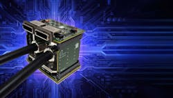
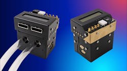
For example, Pactiv transient and DC load testing tools help empower the product development process, accelerating evaluation, characterization, and validation of power delivery schemes (see figure). Providing a platform for comprehensive testing, Pactiv brings together the flexibility and ease of use of the Passive LoadSlammer adapter and the functionality, power, and rise/fall times of the Active FFED solution.
Another is a programmable load cell array that makes it possible to perform fast AC and DC measurements to develop a sophisticated understanding of behavior of a given solution before implementing it into a system. Because LoadSlammer is vendor-agnostic, fair comparisons can be made against various solutions quickly and accurately. Using the LoadSlammer API enables third-party developers to test and optimize a product with minimal interaction from the client.
Mounting time-to-market pressure brings more gravity to the complexity of testing. The ability to emulate the power supply and its transient performance without the actual ASIC in hand is critical to make sure that their power is validated for that product before getting direct support from their distributor or from the manufacturer.
About the Author
Alix Paultre
Editor-at-Large, Microwaves & RF
Alix is Editor-at-Large for Microwaves & RF.
An Army veteran, Alix Paultre was a signals intelligence soldier on the East/West German border in the early ‘80s, and eventually wound up helping launch and run a publication on consumer electronics for the U.S. military stationed in Europe. Alix first began in this industry in 1998 at Electronic Products magazine, and since then has worked for a variety of publications, most recently as Editor-in-Chief of Power Systems Design.
Alix currently lives in Wiesbaden, Germany.


