Demystify Integrated-Phase-Deviation Results In Phase-Noise Measurements
This file type includes high resolution graphics and schematics when applicable.
Most modern spectrum analyzers have an automatic measurement for determining the integrated phase deviation of a mostly sinusoidal signal across a range of offset frequencies. The results can be expressed in units of dBc or rads. The root-mean-square (RMS) phase deviation (in rads) is calculated from the ratio of power of the single-sideband (SSB) phase noise to the carrier (dBc). With a better understanding of how this is done, engineers can both better understand the results and optimize the measurement. To begin, let’s discuss the relationship between the modulating index of an angle modulated signal and the curves of the Bessel function.
Angle-modulated signals, such as carriers with phase and frequency modulation, are characterized by a modulation index (m). The modulation index for a frequency-modulated signal is the ratio of the peak frequency deviation to the modulating frequency. In contrast, the modulation index for a phase-modulated signal is simply the peak phase deviation or Δφpeak. Equation 1 describes this relationship:
Equation 1.
The angle modulating a given carrier frequency, Fc, with a sinusoidal signal at a modulation frequency of fmod, will create an infinite number of sidebands. They will be spaced at frequency fmod around the carrier at frequency Fc. The amplitudes of the modulated carrier and sidebands can be determined by using the modulation index of the signal and the curves of the Bessel function J0 – Jn.
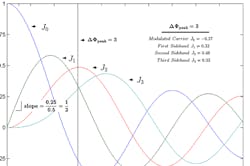
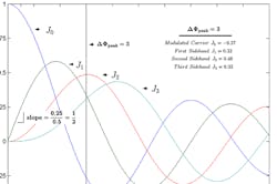
Figure 1 shows the curves of a Bessel function for J0 to J3. A vertical line is drawn at a modulation index of 3, which is equivalent to a Δφpeak of 3 rads. With the intersection of this vertical line with the individual curves of the Bessel function, an indication is given of the relative amplitude of the modulated carrier and sidebands to the unmodulated carrier on a voltage scale.
This example includes the following relative amplitudes:
Modulated carrier J0 = –0.27
First sideband J1 = 0.33
Second sideband J2 = 0.48
Third sideband J3 = 0.33
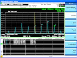
Figure 2 is the spectrum of a phase-modulated signal carrier, Fc, at a frequency of 1 GHz. It has a modulating frequency (fm) of 400 Hz and a peak phase deviation of 3 rads. The amplitude scale is in volts with the amplitude of the unmodulated carrier set to 100 mV. The spectrum of the unmodulated carrier is the yellow trace. The blue trace shows the modulated signal. The marker readouts for the modulated carrier and the first three sidebands are close to the predicted values of J0 through J3. Note that this is the magnitude of the spectrum. As a result, the negative values from the Bessel function are shown as positive.
2. This spectrum of an angle-modulated signal was taken from an Agilent X-Series signal analyzer.
Determining RMS phase deviation from the spectrum of a carrier with sinusoidal phase modulation
In spectrum analysis, there also is a need to determine the Δφpeak k peak phase deviations from the spectrum of the signal. This would be somewhat difficult for large values of Δφpeak. For small values of Δφpeak (Δφpeak k < 0.5 rad), however, examining the curves for the Bessel function will show that the amplitude of the modulated carrier and the unmodulated carrier are close to equal. In addition, the amplitudes of the second-order and higher sidebands are close to zero.
For small peak phase deviations, another advantage is that the first sideband’s relative amplitude is very close to one-half of the peak phase deviation. The Δφpeak of phase noise is very small (<<0.5 rad). To determine Δφpeak using the simple relationship detailed in Eq. 2, it permits these three factors to simply measure the relative amplitude of the first sideband to the amplitude of the modulated carrier:
Equation 2.
where Vss is the amplitude of the single sideband (in voltage) and Vc is the amplitude of the carrier (in voltage).
The amplitude values of most modern spectrum analyzers are on a power not voltage scale. Equation 2 can therefore be used to convert voltage to relative power in Eq. 3. Also, the phase-noise result obtained from most spectrum analyzers is the RMS phase deviation (Δφrms) and not the peak phase deviation (Δφpeak ). Equation 4 converts the peak deviation to RMS. Finally, Equation 5 shows how to determine the carrier’s RMS phase deviation when modulated with a sinusoidal signal and measured on a relative power scale.
Equation 3.Equation 5.
where Pss is the SSB amplitude (in power) and Pc is the amplitude of the carrier (in power).
Calculating the integrated phase deviation from the phase noise present on a carrier
This calculation needs to be tailored so that it can be used to measure the integrated phase deviation from the phase noise. To do this, the term £ (f) is introduced. It is the noise density of the power present in the SSB phase noise of a signal relative to the amplitude of the carrier. The method used to determine the phase noise is the integrated bandwidth method. The user selects a range of offset: the interval fstart to fstop. The power relative to the carrier is then integrated between these two frequency points and computed as shown in Eq. 6:
where £ (f) is in power-density ratio units and ΦSSB is the SSB integrated RMS phase noise (in rads). (Of course, the equation is implemented as a summation—not an integration—in the spectrum analyzer.)
In dBc units, the integrated RMS single-sideband phase noise is:
The power in the two sidebands together is twice as large:
In Eq. 5, it can now be recognized that PSS/Pc is the same single-sideband power ratio computed as ΦSSB. Therefore:
Equation 9 is the calculation made in spectrum analyzers to report the integrated phase-noise measurement results in terms of the RMS phase deviation in units of radians. Now that this has been determined, some simple computations from the RMS phase deviation might be useful in other applications. The jitter (in s) can be calculated by relating the integrated phase deviation to one cycle in time of the unmodulated carrier at a frequency of Fc:
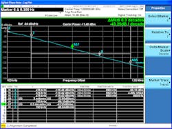
Figure 3 is a display of a log measurement of an unmodulated carrier’s phase noise at a frequency close to 1 GHz (taken on an X-Series signal analyzer). The measurement was set to record phase noise at offsets of 100 kHz to 1 MHz from the carrier. Markers 1, 2, and 3 display the phase noise in units of dBcSSB—rads and s, respectively. Markers 4 and 5 display the slope of the phase noise in units of dB/octave. Similarly, markers 6 and 7 display the slope in units of dB/decade.
3. Shown is an X-Series signal analyzer log plot measurement.
Most modern spectrum analyzers will automate the calculation of the results found in the equations discussed so far. It is beneficial, however, to understand how these equations were derived. After all, it may be useful in better understanding or computing these results, which may not be available in other spectrum-analyzer phase-noise measurements. Some of these also can be automated using built-in band power markers to develop a specific measurement for a task that needs to be accomplished.
Additional Information
Agilent X-Series Signal Analyzers.
N9068A and W9068A Phase Noise Measurement Application, technical overview.
Agilent’s Phase Noise Measurement Solutions, selection guide.
This file type includes high resolution graphics and schematics when applicable.
About the Author
Bob Nelson
MXA (N9020A) Product Support Engineer
Bob Nelson is Agilent Technologies’ MXA (N9020A) Product Support Engineer. He has spent the last 14 years with the company, supporting the Agilent field organization and customers with application-focused measurement requirements. Nelson holds a degree in Electrical and Electronic Engineering from California State University, Chico.


