Tektronix Upgrades Entry-Level Oscilloscope with Xilinx SoC
This article appeared in Electronic Design and has been published here with permission.
What you’ll learn:
- Considerations that Tektronix weighed when evaluating solutions for its new entry-level oscilloscopes
- How Tektronix used Xilinx’s Zynq-7000S SoC to build a more powerful, entry-level family of oscilloscopes
- Specific performance improvements to the new Tektronix oscilloscope since implementing the Xilinx SoC.
Oscilloscopes from Tektronix are designed to allow users to measure the signal integrity of high-speed data buses or the voltage and current in a power supply. An oscilloscope is an indispensable tool for anyone designing, manufacturing, or repairing electronic equipment. It’s often described as “the eyes of engineers” because it allows them to view a vast array of analog and digital signals in both time and RF domains. The challenge is to deliver high performance at the right price point, which often means choosing a hardware platform like an FPGA system-on-chip (SoC).
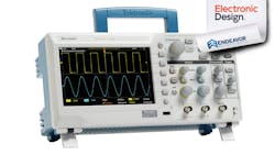
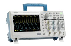
The Tektronix entry-level TBS1000 digital storage oscilloscope (DSO) family targets customers such as educational institutions, small labs, and makers (Fig. 1). The family spans analog bandwidth from 50 to 200 MHz with 1- and 2-Gsample/s rates.
Tektronix was seeking a flexible solution that would enable the company to develop the product quickly at a cost-effective price point. Beyond price, Tek was also looking for a long-term supplier. Its oscilloscope products have been supported in the market for a very long time—typically 10 to 20 years—so it wanted a partner whose products are just as durable. In addition, the company wanted a solution that would allow updates in the field to meet changing customer needs.
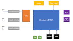
Thus, the design team placed Xilinx’s Zynq-7000S SoC at the center of the TBS1000 platform (Fig. 2). The key aspect of the design is the analog-to-digital converter (ADC) front end created by Tektronix. The SoC enables the oscilloscope to provide a modern set of software and acquisition features in a reduced timeframe and at a price and performance level that’s appropriate for an entry-level oscilloscope.
The SoC serves as the central processing unit running the instrument’s operating system and driving the 7-in. user display. Furthermore, the programmable-logic section of the device interfaces with the on-board ADC to capture and analyze user data.
Choosing a platform that could handle the demanding input signals and be able to provide a graphic user interface (GUI) in a single package is a significant advantage. The SoC made it possible to switch to a new user interface, aligning the TBS1000C with other Tektronix oscilloscopes. What resulted was a significant performance boost as well as an increase in the number of samples from 2,500 points to the current 20,000 points. The new system also improved the waveform capture rate from 500 to 5,000 waveforms/s.
The FPGA allows for more sophisticated signal processing. The family now supports runt trigger mode, which is useful for the analysis of digital signals. A “runt” in a signal is a pulse that doesn’t fulfill some aspect of its dc specification. For example, a signal may not be as high or fall as low as intended. Runts can cause all sorts of problems.
SoC Details
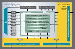
The Xilinx SoC device integrates a single-core Arm Cortex-A9 processor coupled with 28-nm Artix-7-based programmable logic, representing the lowest-cost entry point to the scalable platform (Fig. 3). The integration delivers high throughput between the programmable logic and processing system, providing a huge performance and cost advantage by sharing external memory (DRAM).
The on-chip, high-performance interface between the processor and programable-logic subsystems has also allowed Tektronix to share external double-data-rate (DDR) memory for running the operating system and data capture. This advanced feature saves cost and power without sacrificing performance.
In addition to driving performance enhancements, Xilinx provided comprehensive technical support to Tektronix’s engineering teams. As a result, their local field application engineer could be on site for the initial power-on and debug. Tool training, logic, and PCB design reviews also were provided as part of the partnership.
Resources


