Not an Afterthought: Why Test is Critical in RF System Development

Innovations that increasingly depend on radio frequencies above 5 GHz and up through millimeter wave (mmWave) are shaping the world around us. With advances in technologies such as 5G moving commercial telecom above 5 GHz and up through 28 GHz, 39 GHz, and beyond, frequencies once limited to defense applications are making their way into dozens of new applications. These advances will make roads safer, media and entertainment more accessible, and remote surgeries a reality. But for any of this to happen, engineers and operations teams must overcome challenges inherent to working with such frequencies.
As RF system design demands intensify, more companies look to hire engineering talent that understands RF systems. They discover there’s a limited talent pool of those experienced in designing and testing high-frequency systems while optimizing them for complex applications. This shouldn’t be a surprise; until recently, expertise in 5 GHz and higher frequencies was a relatively niche skill.
Thousands of RF experts aren’t going to materialize overnight, but demystifying the relationship between RF system design and test can go a long way toward successful product development. Many companies outsource their latest RF high-frequency system design for manufacturing, only to realize they’ve waited too long in the development process to avoid common RF test pitfalls. The integration of test procedures into the development process, executed by a team with diverse engineering talent, is crucial to success for products that rely on RF systems.
Testing Matters More than Ever
Often with sub-5-GHz systems, developing RF test procedures was the last step before a product went into full-scale production. These tests were simply a failsafe to keep faulty products out of the marketplace. Design engineers were the real leaders of the development project, while the test team was just seen as a safety net. However, this perceived reality has been flipped on its head as RF design and test moves into higher frequencies to enable complex technologies.
In the current RF system design landscape, test is necessary at every stage in the process. RF design is a costly endeavor, and the ability to optimize a signal is more complicated at higher frequencies. When testing and test development coincide with product development, risk is dramatically reduced.
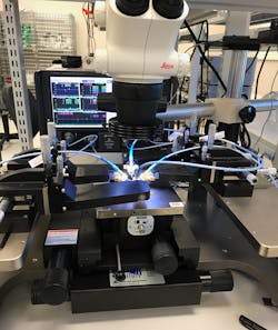
Significant delays and financial setbacks can arise if a company invests a great deal in a design, only to put it on a test bench and discover excessive noise, spurious signals, crosstalk, or efficiency issues are hindering performance. Engineers often think of test as a step that slows everything down, and it can add time to the development process. However, avoiding costly re-design time ultimately gets new products to market faster with better reliability (Fig. 1).

When RF product designs are tested extensively in the prototype stage, critical data is collected for use in further development as well as during production. The testing data is useful for optimizing the design and identifying opportunities to improve signal efficiency, density in microelectronics, or develop algorithms for an automated testing process. Insufficient test during the development cycle eliminates these critical opportunities for enhancing the design.
Failing to incorporate testing can have dramatic results. In a recent survey published in RCR Wireless News, more than 90% of companies that manufacture electronic equipment say that problems related to test-equipment development cost them revenue. More than half of the respondents said that test-development problems slowed the progress of R&D teams at the cost of more than $100,000 per day.1
Design and Test with the Application in Mind
Understanding the challenges in the relationship between design and test is a critical step to optimizing RF products (Fig. 2). RF system designs vary depending on the environment in which the end product will be employed, adding another layer of complexity. Based on whether it’s intended for a satellite, military application, or autonomous vehicle, the way engineers design and test an RF system should change and depends on the environment in which it will be used.

Optimizing size, weight, and power (SWaP) are critical in many products, but even more so for RF systems where the power of the signal can be the difference between success and failure. Original equipment manufacturers (OEMs) want more features and capabilities added to ever-smaller packaging in RF systems. To meet these demands, the design and test teams need to understand the tradeoffs that must be made between power and performance as they miniaturize RF components for various applications.
In this step, performance, power, and efficiency data are critical to identifying the right levers to pull to improve a design. Suppose a specific signal performance is required to meet the needs of an application. In that case, the system design team must understand the power requirements and the implied limitations to size reduction. Electronics size reductions can only go so far in many RF applications, and if designers try and push the limits for a specific application, they may compromise performance.
Achieving this balance requires adequate testing throughout the design process. Test engineers can use the data they gather on performance and power consumption to optimize SWaP and ensure the design team is able to reduce the package size to the lowest point without hindering efficiency and performance. If the design team doesn’t monitor interactions between changes in power and RF signal, but instead builds the product to spec, they may ultimately find out that the size reduction has compromised the RF system’s performance.
Understanding other test processes not related to RF and how they interact with RF systems is another crucial factor for overall system performance. Some standard tests can cause severe damage to an RF system. For instance, implementing a high current or voltage test on an RF system, even common types of in-circuit testing, could destroy RF components.
One solution to this common problem is to use automated test processes designed to respect the sensitivities of RF components. For example, tests can be programmed to respect power thresholds and complete tasks in the correct order so that the test doesn’t damage the RF components. Automated test also ensures reliability and consistency by removing the potential of human error.
Test is an essential element to solving RF system design challenges around the relationship between digital signals and RF signals, which are analog. Digital signals can generate a magnetic field that causes interference with RF signals, but testing processes identify the sources of this type of interference. This data helps the design team understand where to place attenuators within the device to suppress the digital signal and allow the RF signal to transmit without crosstalk or interference.
The Required Investment
Developing RF system test capabilities requires a significant investment in equipment and talent. It requires expensive, highly specialized equipment, isolated test labs, and a team familiar with design-for-test (DFT) techniques and RF design.
A basic test lab setup (Fig. 3) would require:
- High-frequency signal generators
- Signal analyzers and network analyzers
- Specialized RF cables
- Power meters and power sensors configured for high-frequency ranges
- RF couplers, circulators, and a wide range of other peripheral equipment
- Isolated labs and shielded rooms
- Automated test equipment and programming
High-quality talent with specialized expertise and the ability to work in a collaborative team environment is equally important. Successful product development takes teams of specialists in multiple disciplines and processes that incorporate design and test.
Talent and training considerations include:
- Experience in high-end RF equipment
- Capable application engineers that can work with RF designers on new features
- Ability to interpret high-frequency RF test results
- Skill in turning test data into actionable considerations for optimal system design
- Knowledge in signal analysis
Test-Integrated Product Development Drives Results
New applications built on the high-frequency capabilities, from 5G commercial telecommunication networks to autonomous-vehicle operations, will continue to expand. The need for expertise in RF design and test is more important than ever, and the lack of expertise in this area is already a limiting factor in the development of new technologies.
Integrating RF test talent throughout the product-development process makes the best use of this scarce resource. An integrated approach reduces the risk of handoffs between design, engineering, manufacturing, and test, decreasing overall development time and creating optimal RF systems. Talented design and test engineers with experience in RF need to be involved at every stage. Continuous collaboration is truly the key to success.
John Martinez is Manufacturing Test Supervisor at Benchmark Lark Technology.
Reference
1. Hill, Kelly, “Test equipment problems are common and costly, Keysight survey finds,” RCRWireless.com. September 1, 2020.
About the Author
John Martinez
Manufacturing Test Supervisor, Benchmark Lark Technology
John Martinez is the Manufacturing Test Supervisor at Benchmark Lark Technology in Phoenix, Ariz. John has more than 25 years of experience developing and implementing RF test for industry leaders including Intel, TDK, and Qorvo. He first started working in RF systems during his time in the U.S. Army. He holds an Associate's Degree in Mechanical Drafting from Phoenix College.
