This file type includes high resolution graphics and schematics when applicable.
Noise impacts high-frequency systems in many ways, such as transmission distortion and limiting receiver sensitivity of low-level signals. But to accurately analyze noise via modeling with SPICE and other software simulation programs, it must be measured.
The 9812DX wafer-level 1/f noise characterization system from ProPlus Design Solutions Inc. provides new insights into device-level noise with unparalleled 1/f noise measurement speed, resolution, and accuracy. Such wafer-level measurements are critical in various scenarios—for example, semiconductor foundries may seek to enhance the noise performance of a semiconductor process, especially as device geometries shrink to achieve higher-frequency and higher-data-rate operation.
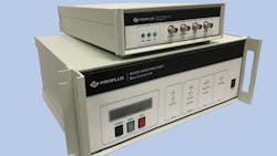
The 9812DX 1/f noise characterization system (Fig. 1) is actually an enhanced version of the company’s widely used 9812D 1/f noise measurement system, with increased resolution and measurement speed (as much as 10 times greater speed and resolution compared to the older system) to accommodate the growing complexity and shrinking device geometries of advanced integrated-circuit (IC) designs.
Of course, the new system isn’t just for foundries: It can also provide invaluable device data for foundry customers looking to improve a process for lower noise levels. In addition, it can give circuit designers more accurate device noise models for evaluating the performance and quality of a foundry process, and for performing accurate noise analysis of their devices.
The noise-measurement system is suitable for process quality monitoring, statistical noise analysis, and studying the effects of process modifications on device and integrated-circuit (IC) noise performance. It speeds and simplifies the collection of device data at different bias points and various other operating conditions, including across multiple die for fast statistical noise data characterization.
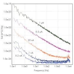
The 9812DX offers a 10-MHz bandwidth, starting at 0.03 Hz for analysis of true wafer-level, low-frequency noise. It can measure the noise of dc current as low as 0.1 nA (Fig. 2) and as high as 200 mA at bias levels up to 200 V. The improvement in noise performance over the older system results in noise measurement resolution of 1 × 10-27 A2/Hz.
The enhanced performance results from an improved system architecture, with redesigned critical subsystem blocks and carefully selected system components. The test system is designed with stable, high-performance components, including a low-noise-voltage amplifier (LNA) with frequency range of 0.03 Hz to 10.0 MHz and 0.65-nV noise at 5 kHz. It also features low-noise-current LNAs covering a frequency range of 0.03 Hz to 10 MHz, and with various resolution and bandwidth options.
The 9812DX 1/f noise characterization system incorporates programmable bias filters, a large number of input/output load resistors for different measurement setups, built-in electrostatic-discharge (ESD) protection for a device under test (DUT), and a built-in GPIB card for controlling additional programmable test instruments.
Another feature is its built-in dynamic signal analyzer (DSA) with large on-board memory and multithreaded processing for improved performance and reduced cost. This eliminates the need for expensive external signal-processing equipment and reduces upfront investment and risk.
In addition to evaluating the noise performance of devices such as field-effect transistors (FETs) and bipolar junction transistors (BJTs), as well as advanced devices like FinFETs, the noise-measurement system is well-suited for analyzing the dark-current noise of photodiodes and optical circuits vital to modern high-speed communications systems and products. It can even evaluate the noise characteristics of resistors from 10 ⦠to 10 Mâ¦.
Finally, the company supports the noise analysis with a number of highly effective modeling and simulation tools, including NanoSpice—a generic parallel SPICE simulator for simulations of extremely dense analog circuits with large numbers of active and passive devices.
ProPlus Design Solutions Inc., 2025 Gateway Pl., Ste. 130, San Jose, CA 95110; (408) 459-6129
This file type includes high resolution graphics and schematics when applicable.
About the Author
Jack Browne
Technical Contributor
Jack Browne, Technical Contributor, has worked in technical publishing for over 30 years. He managed the content and production of three technical journals while at the American Institute of Physics, including Medical Physics and the Journal of Vacuum Science & Technology. He has been a Publisher and Editor for Penton Media, started the firm’s Wireless Symposium & Exhibition trade show in 1993, and currently serves as Technical Contributor for that company's Microwaves & RF magazine. Browne, who holds a BS in Mathematics from City College of New York and BA degrees in English and Philosophy from Fordham University, is a member of the IEEE.


