De-Embed Parasitics from Millimeter-Wave ICs
When characterizing an integrated circuit (IC), it is critical to de-embed parasitics and test-structure features. As RF ICs creep into the millimeter-wave frequencies, small geometries and the need for high-precision measurement techniques have made this task extremely difficult. A team from the University of Grenoble Alpes in France—Vipin Velayudhan, Emmanuel Pistono, and Jean-Daniel Arnould—has compared many de-embedding methods. They also have proposed a highly accurate method based on a half-through approach.
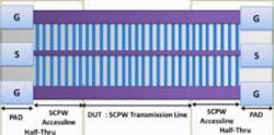
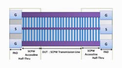
Their half-through method models the probe pads and interconnects using a matrix calculation, which is obtained directly from the S-parameters as test fixtures are de-embedded. This method removes the need to assume symmetry and equivalent models for pad-interconnect parasitics. To create the de-embedding model, three different S-parameter tests must be performed. First, a transmission line with ground-signal-ground (GSG) pads that are 100 μm in length must be tested for transmission and reflection. The same testing is then performed on a GSG transmission line that is 200 μm in length. Finally, a reflection test is performed on a half-through line that is terminated in a non-characteristic load.
The paper discusses the derivation of the equivalent model by converting S-parameters to ABCD matrices. Using the reflection coefficient of the half-through test and signal-flow graph theory, or Mason’s Rule, the researchers then extract the effects of the pads and interconnects referenced to 50 Ω. In comparison to other de-embedding methods, the paper claims that the half-through method outperforms other methods under simulation. The remaining work is to physically implement the half-through method to confirm performance expectations.
See “Half-Thru de-embedding method for millimeter-wave and sub-millimeter-wave integrated circuits,” 2014 10th Conference on Ph.D. Research in Microelectronics and Electronics (PRIME), June 2014, pg. 1.
About the Author
Jean-Jacques DeLisle
Jean-Jacques graduated from the Rochester Institute of Technology, where he completed his Master of Science in Electrical Engineering. In his studies, Jean-Jacques focused on Control Systems Design, Mixed-Signal IC Design, and RF Design. His research focus was in smart-sensor platform design for RF connector applications for the telecommunications industry. During his research, Jean-Jacques developed a passion for the field of RF/microwaves and expanded his knowledge by doing R&D for the telecommunications industry.
