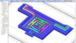
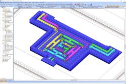
Millimeter-wave frequencies have long been essential to defense-related applications, well before designers starting applying them to automotive safety systems and future cellular network schemes. To develop a broadband receiver based on silicon-germanium (SiGE) semiconductor process technology, the Defence Science and Technology (DST) Group within Australia’s Department of Defence depended on modern computer-aided-engineering (CAE) design and simulation software to help realize a complex circuit and layout (see figure). Specifically, the DST Group used the Analog Office RFIC design software within the National Instruments (NI) Applied Wave Research (AWR) Design Environment.
The SiGe receiver was designed for use from 24 to 45 GHz, with specific performance requirements for noise figure, gain flatness, input third-order intercept point (IIP3), and image rejection across the wide frequency range. The software contains a comprehensive library of accurate device models for use in circuit designs. It also performs electromagnetic (EM) simulation and optimization to allow users to study the predicted results of different circuit components and configurations, even on relatively “exotic” substrate materials such as SiGe.
According to DST Group designer Leigh Milner, “Analog Office provided the design team with a significant advantage. The software’s custom PCells boosted the capabilities of the foundry PDKs, simplifying the SiGe design flow by automating the process to layout complex structures over previous manual methods. In addition to saving engineering time, the new capability helped improve the accuracy of the layouts by eliminating potential data-entry errors.” Semiconductor foundries rely on process design kits (PDKs) to model and simulate different conditions for a semiconductor process, including gate structures for active devices.
About the Author
Jack Browne
Technical Contributor
Jack Browne, Technical Contributor, has worked in technical publishing for over 30 years. He managed the content and production of three technical journals while at the American Institute of Physics, including Medical Physics and the Journal of Vacuum Science & Technology. He has been a Publisher and Editor for Penton Media, started the firm’s Wireless Symposium & Exhibition trade show in 1993, and currently serves as Technical Contributor for that company's Microwaves & RF magazine. Browne, who holds a BS in Mathematics from City College of New York and BA degrees in English and Philosophy from Fordham University, is a member of the IEEE.


