EM Simulation Technologies Support RFIC Development
This file type includes high-resolution graphics and schematics when applicable.
RF integrated circuits (RFICs) employ a variety of different interconnect and passive component geometries. Each requires specialized electromagnetic (EM) technology to provide accurate modeling in a reasonable amount of simulation run time.
For example, a transistor feed network may consist of a complex network of short traces, best modeled using quasi-static techniques for parasitic extraction. On the other hand, electrically longer structures like inter-stage transmission lines and on-chip distributed components such as spiral inductors require planar or 3D EM simulation to capture full-wave behavior. Furthermore, non-planar geometries—e.g., flip-chips, ball grids, and bond wires—require full arbitrary 3D EM simulation.
This article examines the characterization of these different RFIC structures. The EM simulation technology available in NI AWR design software, operating to support component and interconnect modeling within a typical Cadence RFIC design flow, was used.
RFICs vs. MMICs
RFICs are based on silicon or silicon-germanium (SiGe) semiconductor technology, and were originally developed for sub-microwave frequencies. These devices have significantly higher transistor densities than their monolithic microwave integrated-circuit (MMIC) counterparts, which are based on III-V compound semiconductors such as gallium arsenide (GaAs) and gallium nitride (GaN). Targeting high-volume computing and communication applications, RFICs consist of transistor arrays connected by a large number of very short electrical lines, known as “nets,” in a complex network.
These nets are traditionally modeled with discrete resistance and capacitance circuit elements using quasi-static approximations to extract their parasitic effects. Parasitics degrade device performance and, therefore, must be accounted for during simulation.
In EM simulation, quasi-static approximation refers to equations that do not involve time derivatives (static), even if some quantities are allowed to vary slowly with time. The resulting mathematical models can be used to describe traces that are electrically short and thus do not produce significant amounts of EM waves. This EM technique allows designers to account for the impact on performance due to parasitics, providing modeling support for layout complexity with a tradeoff of simpler electrical models.
In contrast, MMICs, which target microwave frequencies and above, utilize traces that are not electrically short. Therefore, they require characterization that includes their full-wave behavior.
Since the layout of the interconnect network itself is a critical part of the electrical design, accurate modeling is required from the design start. Initially modeled using distributed transmission-line theory, MMIC passive components and interconnects are frequently characterized with planar EM simulation using method of moments (MoM) techniques. Such techniques, increasingly being integrated within RF/microwave circuit design tools, can solve large structures.
For example, recent advances in the planar EM simulator AXIEM support fast simulation run times of large networks. As a result, it is now practical to perform EM simulation on an entire MMIC layout directly within an NI AWR Design Environment, specifically Microwave Office, circuit simulation.
Today’s RFIC designs combine MMIC and analog IC structures to achieve the high density/functionality at microwave/millimeter-wave frequencies for emerging communication and aerospace applications. A typical RFIC contains a diverse range of structures requiring electrical characterization, from relatively large spiral inductors to very small high-density interconnects.
Depending on the electrical length of the structure, critical portions of the RF interconnect network may not be adequately modeled through parasitic extraction, requiring the designer to apply full-wave EM simulation. The table describes various EM analysis methods available to create a layout-driven model, along with some of their high-level characteristics.
Matching the Simulator to Modeling Requirements
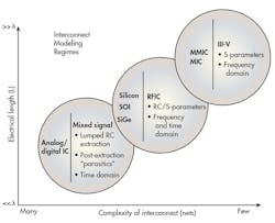
IC modeling requirements are determined by physical length relative to the frequency-dependent signal wavelength (Fig. 1). Distributed models, derived by full-wave EM simulation as opposed to quasi-static approximation, are used for microwave circuits (upper right circle), where transmission lines are electrically long and phase delay must be considered.
Simulating an entire MMIC is a tractable problem for a simulator such as AXIEM, which is capable of solving 100K or more unknowns in less than 30 minutes per frequency point using fast solver technology. Full-wave EM simulators generate S-parameter networks to represent distributed interconnects and passive components in the frequency domain used in most RF/microwave circuit simulations.
EM simulation and modeling requirements for RFIC design fall somewhere between III-V and analog silicon ICs. One design-flow challenge involves applying the appropriate EM simulator to a diverse set of integrated IC technologies, applying parasitic extraction for the active device interconnects, and utilizing a full-wave EM tool for inductors and other structures.
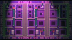
Another challenge for EM simulation design flow is model partitioning. For example, Fig. 2 shows a three-channel RFIC receiver with spiral inductors requiring a planar EM solver like AXIEM or the “Analyst” 3D finite-element-method (FEM) solver.
In this receiver, the designer may choose to model each of the matching coils individually, all of them together in a single channel, or all channels in one big simulation structure. The choice will significantly impact EM simulation speed and may or may not affect the overall accuracy, depending on the coupling that occurs between individually modeled components.
Comparing EM Simulation Techniques
Parasitic Extraction
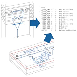
In traditional parasitic extraction, a netlist is created using EM quasi-static methods applied to the physical layout of the nets/traces (Fig. 3). The resulting model is the resistance of each net and the self-capacitance of each net to ground. Mutual capacitances between nets can also be included.
One modeling challenge is properly identifying the ground. In general, silicon chips do not have a well-defined ground. RFIC grounds can be formed by the doped substrate of the silicon, or a specially constructed interconnect. Spirals often have a metal grid under them or a surrounding guard ring to provide a ground and associated current return path. While the extra metal adds capacitance, which affects the performance of the circuit, the explicit ground improves model accuracy, thereby reducing potential design failure. Some parasitic extractors can calculate partial inductance for higher frequencies, but will yield inaccurate results unless the entire current loop is correctly defined.
Automated-circuit-extraction (ACE) technology provides circuit extraction within the NI AWR Design Environment, extracting nets as distributed models for structures such as transmission lines and vias. ACE models interconnects using a series of transmission lines, resistors, and even coupled transmission-line models for parallel traces, as shown in Fig. 3.
ACE extends RLGC parasitic extraction methods to support electrically longer lines for critical nets as an alternative to planar EM simulation. However, the accuracy of the extracted distributed models depends on a well-defined ground and associated current return.
Cross-Sectional (2D) Quasi-Static Solvers
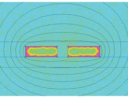
A quasi-static cross-section (alternatively known as 2D) simulator solves cross-sectional slices of the IC technology’s substrate and trace construction (Fig. 4). This simulation technique solves for the capacitance of the structure and then calculates the frequency-dependent inductance and resistance.
Indeed, a simplified form of this type of solver is used in the static capacitance matrix in the previously mentioned parasitic extractors. The more sophisticated version shown in Fig. 4 includes all frequency-dependent effects, such as lossy silicon substrates, and is used in some of NI AWR Design Environment’s built-in silicon transmission-line models.
This fast simulator runs seamlessly in the background. Of course, the designer still can either explicitly model the interconnect as a transmission line or use ACE to extract the transmission-line models. Once created, the cross-sectional solvers ensure that the line model is accurate, provided the cross-section was accurately defined.
Method of Moments (Planar)
MoM is a frequency-domain solution that meshes conductors only and uses Green’s functions to calculate the effect of conductor currents on each other (Fig. 5). In RFIC applications, MoM solvers are typically used for distributed lines connected by vias, where modeling phase delay is critical. Examples include spiral inductors, branches, discontinuities, and long-line sections between active devices.
One consideration for MoM simulators modeling silicon relates to the common use of aluminum for the RFIC’s top metal layers. Typically, MoM simulators characterize loss using an impedance boundary condition on the surface of the metal trace. MoM simulators do not solve for currents inside the trace, which can lead to inaccuracies in the simulated resistance. This shortcoming is most critical in accurately calculating the Q of a spiral inductor. Therefore, Q measurements of a spiral inductor should be performed with a full 3D EM simulator such as Analyst, which will provide a mesh inside the metal and lead to a more accurate result.
Finite Element Method (3D)
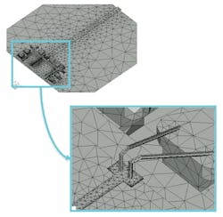
Analyst uses FEM to produce a volumetric mesh for solving for the electric fields using Maxwell’s Equations (Fig. 6). Analyst also addresses completely arbitrary structures such as wire-bond/bond-pad interfaces. However, the technique takes longer to simulate and has the largest memory requirements of all EM simulators mentioned.
Given the complexity of RFIC design, EM simulation is most effective when integrated within a design flow that includes circuit simulation, optimization, corner/yield analysis, and process design kit (PDK) support. Designers using multiple EM techniques for model creation must be able to easily swap simulators or compare the results from different simulators to determine the best method for a given structure. Swapping various model types between extracted nets, EM-derived S-parameters, and more complicated RF models is easily handled in Microwave Office using the switch lists feature.
Supporting multiple EM technologies within a single project or circuit hierarchy is necessary for simulating heterogeneous RFIC structures simultaneously without having to import models from third-party EM tools. As an example, NI AWR Design Environment supports circuit co-simulation in Microwave Office (or Analog Office) with critical flip-chip transitions extracted with Analyst, spiral inductors simulated with AXIEM, and nets representing a complex transistor feed network modeled in ACE.
Circuit/EM Co-Simulation
Embedding layout-driven EM simulation into a circuit hierarchy that combines a model of all significant IC structures with the remaining active/passive components will provide greater accuracy for design verification. Figure 7 shows an RFIC design verification with the active devices connected directly to the EM simulated layout using in-situ ports. This circuit setup and simulation is made possible through the internal ports and de-embedding capabilities within AXIEM. De-embedding lines remove artificial interactions between the simulation port and nearby elements of the EM structure.
Accurate EM/circuit co-simulation requires specific capabilities on behalf of both the circuit and EM simulators. Circuit simulations for RFICs are often conducted in both the time and frequency domain. The transient circuit simulator in Microwave Office performs time-domain circuit analysis, while large-signal frequency-domain circuit analysis is performed through harmonic balance.
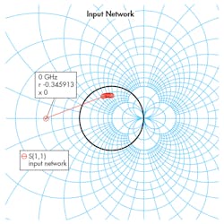
Accurate harmonic balance results need broadband network impedance information at all transistor nodes, including dc, excitation frequencies, and harmonic frequencies. Incorrect dc impedance will result in a transistor biasing discrepancy, while incorrectly defined harmonic terminations will impact the in-band transistor results. Incorrect dc impedances occur when S-parameters are improperly extrapolated to f=0, as shown in the example in Fig. 8.
Certain EM techniques, such as FEM, are ill-suited for extracting low-frequency and dc impedances. Analyst has a low-frequency limit of 10 MHz, whereas the AXIEM simulator has a built-in low-frequency solver that can address modeling problems at dc. For parasitic extraction at dc, the designer should use AXIEM, ACE, or a third-party EM solver accessed through NI AWR Design Environment’s EM Socket. By having easy access and flexibility in the use of diverse EM technologies, RFIC designers can address a vast array of different structures with electrical models that produce accurate circuit simulations.
EM simulators maintain one key advantage over test equipment—they have greater flexibility in the placement of a measurement port than is physically possible with a vector-network-analyzer (VNA) test port. However, port validity and de-embedding of RFIC structures can encounter problems as the number of ports increase due to the close proximity of ports to each other, reducing the isolation and increasing the modeling error. Defining the proper ground reference is also critical to avoiding discrepancies between measured and modeled results.
Conclusion
Multiple EM simulation technologies are available to model the wide variety of geometries and electronic packaging used in today’s RFICs. Designers should be aware of which technology is best suited for modeling a given structure, factoring in criteria such as speed versus accuracy. NI AWR Design Environment and EM Socket provide a platform for integrating multiple EM technologies and circuit co-simulation with Microwave Office. The tools give designers the ability to explore their modeling options using AXIEM, Analyst, and ACE EM solvers or third-party solutions to effectively manage an EM-centric RFIC design flow.
David Vye is Director of Technical Marketing; Dr. John Dunnis Electromagnetic Technologist; and Dr. Jim Carroll is Director IC Design Flows for National Instruments, AWR Group.
Recommended reading:
John Dunn, “Interconnect Modeling and Simulation for RFIC Design,” RF Globalnet, February 2007.
Juergen Hartung, “Interoperability Enables a Complete RFIC/Package/Board Co-Design Flow,” Microwave Journal, July 2014.
James C. Rautio, "Perfectly Calibrated Internal Ports in EM Analysis of Planar Circuits,” IEEE IMS, 2008.
About the Author
David Vye
Technical Marketing Director, Cadence
David Vye is the senior product marketing manager for AWR software at Cadence, where he’s responsible for product messaging and positioning in the RF/microwave market. A former editor and business development manager for Microwave Journal, David has held a number of technical and marketing positions throughout the RF/microwave industry. He holds a BSEE from the University of Massachusetts at Dartmouth, with a concentration in microwave engineering.
