Advanced Design Tools Support Waveform-Engineered High-Efficiency Power Amplifiers
This file type includes high resolution graphics and schematics when applicable.
Engineers designing today’s wireless handheld devices and infrastructure equipment are accustomed to accurate, reliable simulation tools. However, they recognize that power amplifiers (PAs) are among the last types of circuits to reach the point where the simulation can be regarded the same as a laboratory prototype. The purpose of this paper is to show how NI AWR Design Environment can be used to both accelerate the design process and improve the performance of PAs using the latest device technology and the most recent developments in high-efficiency switch-mode classes of operation.
Introduction
The ongoing evolution of wireless networks has required significant advances in power amplifier design. High-efficiency PAs are needed to reduce power consumption in wireless infrastructure equipment, from wide area rural base stations to the smallest femtocells. Reduced power consumption does much more than save energy—it minimizes waste heat, increases reliability, and enables smaller size equipment enclosures. These advantages are invaluable since much of the equipment for 4G wireless system expansion is being installed in remote locations or confined spaces with limited access for maintenance. Also, both new and existing sites are increasingly using alternative power sources like solar panels, wind turbines, and other environmental energy harvesting methods to provide backup (or primary) power.
Achieving High Efficiency
The highest efficiency power amplifiers use switch-mode operation—Classes D, E, F, and others. Earlier modes of amplification (Classes A, B, and C) are defined by the conduction angle established by the bias point, and are driven with sine wave signals. Switch-mode PAs are all biased at the turn-on threshold and driven either with square wave signals or with sine waves with sufficient amplitude to switch the power device almost as quickly as true square waves. The output of an ideal switched power device is also a square wave, which contains significant energy at harmonics of the fundamental frequency. The various classes of switch-mode amplification are defined by the way the output network deals with the harmonics, e.g., whether they are terminated with an open or short circuit. The operation of each class corresponds to a particular voltage and current waveform at the output terminal of the power device.
Finally, these PAs are used with advanced linearization techniques such as envelope tracking, outphasing, and digital predistortion, and must have reliable, repeatable designs that require minimum adjustment on the assembly line and have stable performance in the field over their operational lifetime.
Simulation tools are an essential part of the design process for switch-mode PAs. To achieve maximum performance, the designer must have tools that support design and optimization to obtain the desired voltage and current waveforms. Circuit simulation, thermal analysis and board layout for RF and DC must all be done in concert, with accurate results. Design shortfalls must be identified and quickly resolved in simulation, before any hardware is constructed—competition and rapidly changing technology simply do not allow multiple prototype iterations. The simulation platform must include robust mathematics, highly accurate device and circuit element models, and must have operational features that support an engineer’s design effort in the same manner as the best prototype shop and test bench.
Class F and Inverse Class F PA Design Using Microwave Office
Class F and Inverse Class F amplifiers are a relatively new development and have generated considerable interest among PA designers. As noted above, switch-mode PA outputs have significant harmonic content, and Class F amplifiers attempt to leverage the power in the harmonics to increase efficiency. A perfect Class F amplifier will have a square voltage waveform at the drain-source terminal pair and a corresponding half sine waveform for the current.
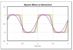
With these ideal waveforms, Class F can theoretically produce 100% efficiency, since there is no simultaneous current and voltage that results in dissipated power. However a perfect square wave is comprised of an infinite number of harmonics, which is an impractical solution. Fortunately, we can use a Taylor series expansion to explore the quality of the waveform versus the number of harmonics used (Fig. 1).
In a basic Class F PA, the input-matching network is typically designed to provide the best match for power gain and the output network is designed for a match at the fundamental, while managing the harmonics. There is a series-tuned resonator in the RF output line to pass the fundamental frequency and a quarter wave shunt element in the bias line that presents different impedances to even and odd harmonics.
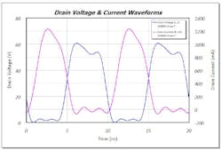
With this basic Class F circuit configuration and a default setting in the harmonic balance simulator that considers five harmonics, the waveforms obtained are shown in Fig. 2. The blue voltage waveform approximates a square wave and the magenta current waveform approximates a half sine wave. Although these waveforms are not ideal, the simulation results predict a drain efficiency of slightly more than 81% at an output level of +24 dBm. The gain is significantly compressed at that high efficiency point.
Inverse Class F, as the name implies, has opposite voltage and current waveforms. The same schematic also represent this class if the waveforms were reversed, e.g., a half sine voltage waveform and square current waveform. The way harmonics are handled is also reversed. For the same Cree GaN HEMT in an Inverse Class F mode of operation, the input-matching network is basically the same and the output network still has the series-tuned resonator, but the quarter wave transmission line is moved from the shunt bias line to the RF output line, where it again is used to manage the harmonics.
Waveforms obtained for this instance reveal a square wave for current and a half sine wave for voltage waveform. The drain current measurement swings below zero due to circuit parasitic effects. With this operating condition, the maximum efficiency of the PA reaches 87%.
This file type includes high resolution graphics and schematics when applicable.
Fundamental and Harmonic Load Pull using AWR Load Pull Wizard
This file type includes high resolution graphics and schematics when applicable.
To take the next step in design, engineers can use a powerful feature in Microwave Office, the Load Pull Wizard. The PA designer must simultaneously find the most efficient impedance match at the fundamental while properly terminating each harmonic with the necessary short or open circuit. It would be extremely time consuming to run a series of laboratory load pull tests to determine the impedances at fundamental and harmonic frequencies which will result in the proper I and V waveforms. The ability to use load pull simulation to determine these impedances greatly speeds and simplifies the design process.
The first task is to do determine input matching with a source pull for power gain and power-added efficiency. At this point, the output of the transistor is simply terminated directly into 50 ohms. For output matching, a fundamental frequency load pull is performed, again for power gain and PAE, using the source pull results at the input of the device. Then the second and third harmonic terminations are loaded into the load pull wizard and the load pull tuners set either to arbitrary values or to the values in the basic circuits above for Class F or inverse Class F. Then second and third harmonic source pull and load pull will be invoked with the wizard to find the optimum impedances for best power gain and PAE.
When second and third harmonic terminations are included, their impedances may affect the fundamental impedance. Consequently, it will be necessary to iterate the load pull sequence at least twice to get to that optimum point. Transistors and matching networks using practical lumped and distributed components are not perfect, and some waveform engineering will actually be done via the Load Pull Wizard to peak up the efficiency power and gain.
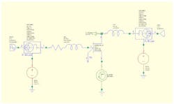
Figure 3 shows the basic setup for a series of load pull operations on a basic PA circuit. A source pull tuner is on the left, a load pull tuner is on the right, and bias tees have been integrated into those tuners as well. The CGH40010F GaN HEMT device is a bare die, so wire bonds are included in the simulation.
The first fundamental source pull for gain achieves 15.3 dB at the optimum point, which is automatically calculated through all the converged points. The source pull for output power results in a maximum of 43.5 dBm. Finally, the fundamental source pull for power added efficiency, results in an optimum point at an impedance that is very close to the maximum for both gain and power. This simplifies the matching task considerably and even though the load is directly into 50 ohms, the PAE is already over 60% at this point.
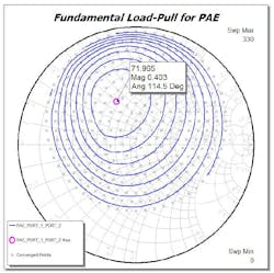
For load pull simulation and optimization, the source pull is set at the impedance that provided the best PAE. The fundamental load pull results for gain, then for power are similar, and fundamental load pull for PAE does not result in a large change. Figure 4 shows the PAE results, which is improved from 60.5% with source pull only to 72%. At this point both ports are matched for PAE only at the fundamental.
With the fundamental source and load pull set to previous values, the wizard can find the optimum second harmonic load pull for maximum PAE. The PAE has improved to over 80%. The third harmonic load pull has a smaller effect, providing between one and two percentage points improvement in efficiency. Of course, the design goal for optimum harmonic impedances could also be power gain or output, as needed for the particular application.
Now that the required optimum fundamental second and third harmonic terminations have been identified, matching networks can be synthesized to emulate the required impedances as closely as possible over the complete frequency range. This simple case is a relatively narrow band design centered at 2 GHz. Remember that practical networks will approximate, but not exactly match, the impedances that have been defined by the load pull data.
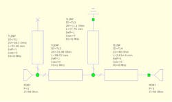
Figure 5 is a synthesized Class F input network, which in this case consists of transmission lines, a short-circuited stub on one side and an open-circuited stub on the other. The S11 of this input network at fundamental and harmonics does not exactly match the values determined by the input source pull, since its design is limited to available components and practical distributed elements.
The resulting synthesized Class F output network is similar to the one in the basic design circuit. The quarter wave line also provides drain bias to the transistor. In addition there is an open circuit stub that provides a transmission line transformation resulting in an open at the second and a short at the third harmonic.
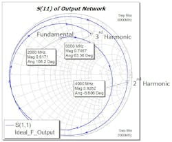
Looking into the input of the network where the drain of the device would be, Figure 6 shows the fundamental, second and third harmonic impedances. Again, going back to the wizard, it can be seen that there are some differences between the practical transmission line-based network and the ideal impedances determined by load pull.
The complete circuit with the transistor and bias voltages can be simulated as a whole. Simulation results for power gain, output power, and PAE reveal that the PAE reaches 84%, which is slightly better than predicted by the Load Pull Wizard results.
As for the waveforms of the drain voltage and current, recall what was noted earlier—when source and load pull are done with the Microwave Office wizard, users will get some degree of waveform engineering. If they tell the wizard that they want to have maximum PAE, the wizard’s optimization algorithm will try to produce the voltage and current waveforms at the transistor that are not only the right shape but also ideal and anti-phase. It can be seen that the half sine voltage waveform is close to being a half sinusoid, although the current waveform deviates from being square. Again the current goes negative because measurement is not at the intrinsic device terminals.
The process of simulating source pull and load pull at the fundamental frequency and harmonics replaces many such tests on the workbench. The Load Pull Wizard has the added value of a final optimization with practical element values obtained by matching network synthesis, with the goal of obtaining the desired voltage and current waveforms.
A Note on Models
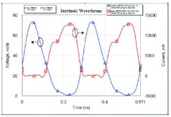
Subsequent to the work described in this paper being done, Cree has developed a new set of device models with two additional test ports that effectively de-embed device parasitics and allow observation of the drain voltage and current waveforms as if probing directly on the die.8Figure 7 below shows a drain waveform using the new model, clearly showing minimal current excursion into the negative region (red trace). Of course, when setting up a simulation the designer must account for parasitics due to transistor mounting and connection to external traces and components.
2 GHz Class F PA Example
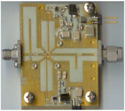
A practical example is based on work originally done by Schmelzer.2 The Cree device used is again a CGH40010F GaN HEMT bare die in a 2 GHz design. In addition to the basic Class F topology that was previously discussed, this particular design also uses shunt resistors in the input network, which serve to stabilize the network.
At the output network is the shunt quarter wave transmission line, also used for bias, along with the series tuned resonator and the transmission line terminations just described.
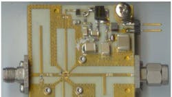
Figure 8 is a photograph of the circuit that was actually built for this design.
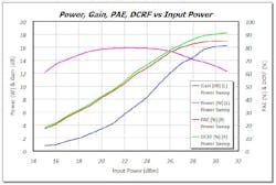
Figure 9 shows the measured results. Gain is in magenta, power is in blue, PAE is red, and the green curve is DCRV or drain efficiency. These results are in good agreement with the simulated performance.
Conclusions
This and other successful designs demonstrate the validity of PA design aided by Microwave Office’s Load Pull Wizard, synthesis of matching networks, and final optimization to obtain voltage and current waveforms that are as close as possible to the ideal for the class of operation, such as Class F and Inverse Class F.
Engineers can now take advantage of accurate simulation tools with the right set of features for effective PA design. Combined with advanced device models from device manufacturers and continued refinement in switch mode amplifier circuits, new PAs for wireless infrastructure and other applications can be developed quickly, with very high efficiency and reliable, repeatable performance.
References
1. P. Colantonio, F. Giannini, E. Limiti, High efficiency RF and microwave solid state power amplifiers, John Wiley & Sons, Ltd, 2009.
2. D. Schmelzer, “A GaN HEMT class F amplifier at 2GHz with >80% PAE,” IEEE Journal of Solid-State Circuits, Vol. 42, No. 10, Oct. 2007.
3. A. Grebennikov and N.O. Sokal, Switchmode RF Power Amplifiers, Newnes, 2007.
4. V.A. Borisov and V.V. Voronovich, “Analysis of Switched-Mode Transistor Amplifier with Parallel Forming Transmission Line”, Radiotekhnika Elektronika, vol. 31, pp. 1590-1597, August 1986.
5. M. K. Kazimierczuk, “A new concept of Class F Tuned Power Amplifier,” Proc. 27th Midwest Circuits and Systems Symp., pp. 2007-2012, November 1997.
6. T. He, “Design of Radio Frequency Power Amplifiers for High Efficiency and High Linearity,” A Thesis Presented to the Faculty of California State University, Chico, 2009.
7. A. Grebennikov, “Load Network Design Technique for Class F and Inverse Class F PAs”, High Frequency Electronics, pp. 58-76, May 2011.
8. R. Pengelly, W. Pribble, and T. Smith, “Inverse Class-F Design Using Dynamic Loadline GaN HEMT Models to Help Designers Optimize PA Efficiency,” IEEE Microwave Magazine, September-October 2014.
This file type includes high resolution graphics and schematics when applicable.
