A Top Down Methodology for Silicon-Platform Optimization
This file type includes high resolution graphics and schematics when applicable.
Recently there has been an explosion of short range wireless applications. Some well-known examples include NFC payment systems, wireless charging, and more. These applications require an interaction of electromagnetism (EM), electrical, and mechanical domains. Unfortunately, there is no tool which can computationally solve the complete system efficiently for rapid silicon applications and system specifications. The net effect is that either the silicon is not properly specified or the system needs to be redesigned.
Traditional electrical simulators such as Spice are effective in solving lumped element equations. However, such tools cannot model EM fields present in sensors, especially when they are embedded in the vicinity of other components and a metallic chassis. Other products can solve Maxwell’s equations using finite-element methods (FEM) but are woefully inefficient in importing transistor parameters.
This article presents a unified methodology which takes into account the best of both tools, creating a top-down view of a complete system. A representative system is used in demonstration, but this methodology can be extended to other interdisciplinary optimization problems.
Methodology
One application could involve sending a PCIe clock over a contactless system. Traditional PCIe clocks propagate from a system-on-chip (SoC) over FR4 traces to a PCIe card. There is a wealth of literature using signal integrity tools to model this effect. However, in this scenario a docking connector for a hermitically sealed tablet is considered where PCIe signals are to be transmitted over a short-range wireless link.
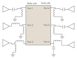
This scheme allows for more rugged tablets with no exposed contacts. Pads on the tablet capacitively couple to corresponding pads on the docking connector and enable PCIe signal and clock information to be transmitted across the wireless link (Fig. 1). The big question is how to model the contactless system and specify the silicon parameters to still meet the PCIe specifications.
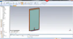
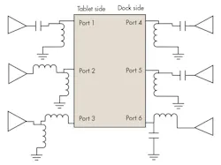
A 3D EM solver (CST Studio) is used to create a network model for the system—without the driver, which is in silicon (Fig. 2). A six-port S-parameter reciprocal network is extracted from the full wave simulations (Fig. 3). Ports 1 , 2, and 3 are considered part of the tablet, while ports 4, 5, and 6 are considered part of a dock. As such, S14 or S41 would provide the path loss for signals traveling from one PCI trace to the corresponding trace on the dock.
S12 would provide the coupling between ports on the same tablet device and has to be minimized to reduce cross talk. Conceptually, Ports 1, 2, and 3 can be considered drivers, with ports 4, 5, and 6 being the receivers. That being said, reciprocity ensures the link is identical in the opposite direction from the dock to the tablet.
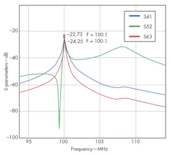
Optenni Lab (a matching circuit generation program) was used to retrieve optimal matching values for all the ports (Fig. 4). It is seen that matching leads to a minimization of losses at the target frequency of 100 MHz (PCIe clock spec). The matching tool outputs a requirement of 55-Ω driver impedence. This then forms the basis of silicon specification.
Once the impedence matching required for maximum power transfer through the link is known, it is feasible to specify the silicon parameters. In addition, a sensitivity analysis can be performed to measure the range required on the impedance—to account for both silicon skew as well as system varation over manufacturing tolerances, temperature, humidity, voltage, and more.
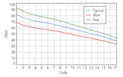
In order to model the silicon an electrical simulator Spice is required. Spice allows a transistor level representation of the driver, which can take the device level parameters into account. It can also do a much better job modeling manufacturing tolerance, voltage, and other factors. The desired impedence range also enables the right architecture for this application (Fig. 5).
Lastly the transistor level model can be assembled with the s2p model of the link to build a complete end to end system. This enables a non-linear transient simulation to be performed to measure slew rates and large signal reflections.
Conclusion
The continuing advances in both silicon modelling, circuit simulators, and 3D EM simulators have meant that increasingly a design team has access to simulation and computer tools. These tools allow for a robust co-design of silicon, PCB, and system design. This article uses a hypothetical example of transmitting PCI-e clock over an air interface to describle one such co-design possibility using Spice for circuit modelling, CST for 3D EM modelling, and Optenni for impedance matching.
The rapid miniaturization of consumer devices coupled with the use of challenging materials such as an all-metallic chassis and severe-power-consumption constraints has meant that complete system design is required to converge on performance targets. The maturation of computer tools across the workflow has meant that there are multiple off the shelf tools to accomplish this co-design flow. These tools are available even for traditionally low cost designs, such as those used for consumer devices, tablets, phones, and wearables.
This file type includes high resolution graphics and schematics when applicable.
About the Author

Leaders relevant to this article:
