Multi-Die Systems Reshape Semiconductor Innovation
This article appeared in Electronic Design and has been published here with permission.
What you’ll learn:
- What makes up a multi-die/chiplet system?
- What’s driving demand for multi-die systems?
- The challenges of multi-die system design.
Demands have never been higher for—and on—semiconductors. From smart speakers to self-driving cars and robotic manufacturing equipment, chips are elevating our smart everything world to new heights. In 2021, the semiconductor industry marked a record by shipping 1.15 trillion chips. Increasingly, as applications become more intelligent, these chips are being asked to deliver much more processing prowess, better power efficiency, and, for space-constrained designs, smaller footprints.
It’s a promising and exciting time for the electronics industry, with transformer models, generative artificial intelligence (AI), and immersive experiences creating unprecedented demand for compute and data rates at ever lower power levels. As a result, new players are entering the chipmaking landscape and bringing to life innovations that are transforming the way we learn, work, play, and, when you think about it, live.
However, all of these chipmakers are facing deep limitations as Moore’s Law slows, particularly for designs targeting compute-intensive workloads.
The reality is, migrating traditional, monolithic semiconductor designs to smaller process nodes is no longer generating the benefits that such scaling once did. And attempting to do so will even hit manufacturing walls.
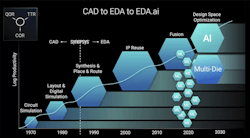
To meet the challenges of scale as well as systemic complexity, more chipmakers are turning to multi-die systems. An interdependent architecture that provides integration of heterogeneous dies, or chiplets, in a single package, multi-die systems enable accelerated scaling of system functionality (see figure).
Designers can also reduce risk and time-to-market, lower system power, and more quickly create new product variants. Multi-die systems are becoming the system architecture of choice for applications like high-performance computing (HPC), autonomous vehicles, mobile, and hyperscale data centers.
This article examines the main drivers of multi-die systems, how they can generate bottom-line benefits, and how they’re moving innovation forward. Read on to understand the essentials of a chip architecture that’s shaping the semiconductor industry.
What Makes Up a Multi-Die System?
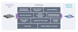
Rather than a single SoC consisting of a processor, memory, and I/Os, a multi-design system is all of this and much more. Inside a single advanced package, you’ll find multiple dies—potentially on different process technologies and for different functions.
There are different approaches to creating such a system. Disaggregation is one approach, whereby a large die is partitioned into smaller dies to enhance system yield versus monolithic dies. An example of a disaggregated, heterogeneous design is an automotive system in which different dies in the package are designated for disparate functions, such as sensing, object detection, and general compute. The disaggregated approach can also be applied to a homogeneous design, such as one that’s disintegrated into multiple instances on the same compute chiplet.
Furthermore, multi-die systems can be developed by assembling dies from different process technologies to achieve optimal system functionality and performance. An example is a system with dies for digital compute, analog, memory, and optical compute, each at a process technology that’s optimal for its function.
Dies in multi-die systems can be placed side-by-side or stacked vertically in a 2.5D or 3D package. Advanced packaging technology, along with interconnect standards like Universal Chiplet Interconnect Express (UCIe), are helping to usher in this new era of chip design.
What’s Driving Demand for Multi-Die Systems?
The late Gordon Moore’s 1960s observation that chip density would double every 18 to 24 months has continued to drive innovation in the semiconductor industry. However, increasing systemic and scale complexities are pushing the limits of Moore’s Law.
Compute-intensive applications like hyperscale data centers and AI/machine learning (ML) are flourishing, while the data itself has become more complex given the emergence of bandwidth-hungry machine-to-machine communication. Massive SoCs with trillions of transistors can support some of these applications.
But as die sizes hit the reticle limit of the manufacturing equipment, adding more transistors to support application demands requires adding more chips, which leads to impossible-to-achieve die sizes. There’s also a steep learning curve to ramp up production for desired yields.
Multi-die system architectures provide a way to address the learning curve, along with yield and silicon cost concerns. Not every function needs to be on the most advanced process node. By mixing and matching dies from older technologies with those on more advanced nodes based on their targeted functions, design teams can reap the benefits of a better performance/cost ratio as well as better yields.
There are also manufacturing advantages, because multi-die systems don’t involve the very large dies that come with greater yield risks. What’s more, by reusing silicon-proven dies, designers can speed up time-to-market for their systems.
The convergence of four key drivers is moving the needle toward multi-die systems:
- Growing functionality: In the face of reticle limit challenges, applications are demanding higher bandwidth, lower latency, and substantially greater compute performance.
- Power predicaments: Splitting up a large design can more effectively address the power requirements that vary based on target functions.
- Opportunities to serve multiple end markets: Optimized, modular architectures provide a faster way to develop product variations and, thus, capitalize on multiple business opportunities.
- Cost: Achieving the level of yields for the types of chips that can address today’s complexities has become prohibitively expensive.
Companies that haven’t traditionally designed their own chips are now doing so, in the interest of achieving differentiation for their unique market requirements.
From the digital behemoths creating immersive online platforms to hyperscalers building out massive data centers and AI innovators developing the next intelligent product, these companies are in many ways driving the evolution of multi-die system architectures. AI companies may seek a specialized architecture to boost performance of ML algorithms, while a hyperscaler might want to find the ideal power/performance balance to support compute-intensive workloads and operate as energy efficiently as possible, for instance.
What are the Key Challenges to Designing Multi-Die Systems?
The shift from monolithic SoCs to multi-die systems can be likened to the move from hand-drawn schematics to RTL and synthesis so many decades ago. The latter was made possible by electronic design automation (EDA) technology, which brought software and hardware solutions to automate the flow to design and verify chips. Today, advances in chip packaging technologies and the emergence of industry standards such as HBM3 and UCIe are enabling heterogeneous integration of dies.
On the packaging front, there are a variety of types to choose from, based on advantages in performance, area, and connectivity, including silicon interposers, redistribution layer (RDL) interposers, fan-out wafer-level packaging, and hybrid bonding.
As for the standards, they help to ensure quality, consistency, and interoperability. HBM3 provides high-capacity memory, preventing memory bottlenecks in 2.5D multi-die designs. UCIe is fast becoming the de facto standard for die-to-die interconnects, providing the bandwidth, low power, and low latency for package-level integration of chiplets.
The challenges involved in developing multi-die systems balloon due to the interdependencies in these complex systems.
With so many interconnected components, multi-die systems are best considered from a system-wide perspective. A co-optimization approach that simultaneously addresses the system, the dies, and the package can help optimize performance, power, and cost.
But, as with any complex system, many questions arise: How should the dies be split? What’s the best type of packaging to use? How do you ensure that your system will perform as intended? How do you develop such a system under aggressive time-to-market targets. And so on.
Every decision and every choice in the architecture of a multi-die system must be made with consideration of each component, as well as the impact on the system’s overall power, performance, and area (PPA) goals. Multi-die system design teams stand to generate the best results by addressing all of the challenges together via a holistic approach. After all, the heat that one die dissipates could impact the performance of the die next to it.
Similarly, what happens at the front-end logical design must account for the back-end physical design. Without a holistic approach, engineers risk encountering time-consuming and costly iterations.
What is the Way Forward for Multi-Die Systems?
As the semiconductor landscape continues to evolve, it’s clear that design teams will need flows and tools that are tuned to the unique challenges of multi-die system architectures. Stitching together disparate design and verification tools won’t be effective in this realm. The end goals remain similar to those for monolithic SoCs: Teams want to optimize PPA while enhancing their productivity and meeting time-to-market targets.
Given the multi-dimensional nature of multi-die systems, what’s needed is a comprehensive and cohesive solution that can scale and is optimized to handle the complexity of these types of designs. The ideal solution would enable early architecture exploration, rapid software development and validation, efficient die/package co-design, robust and secure die-to-die connectivity, and improved health and reliability of the system.
To achieve the promise of multi-die systems, the process to develop them must be holistic in nature, taking into account all of the interdependencies inherent in this type of chip architecture.
For every immersive escapade in the metaverse, each function that a car can perform on its own, and every time a machine is able to anticipate what you might want, the underlying system is asking the silicon chips inside to deliver a lot and in real-time. Compute-intensive applications such as virtual reality/augmented reality, autonomous cars, and AI will continue demanding ever-greater performance, bandwidth, and area benefits.
Multi-die systems present a way forward to meet those challenges head on. In fact, the next wave of semiconductor innovation—sparking the transformative products that are enhancing our modern world—is riding on them.
For more information, download How Quickly Will Multi-Die Systems Change Semiconductor Design?
About the Author
Shekhar Kapoor
Sr. Director of Product Management, Synopsys EDA Group
Shekhar Kapoor is Sr. Director of Product Management at Synopsys, responsible for multi-die system design and digital platform and analytics solutions. He has over 20 years of professional experience, managing the design realization and signoff products at Synopsys. Prior to that, he had leading design and application engineering roles at LSI Logic (now Broadcom) and IBM.
Shekhar holds an M.S. degree in Electrical and Computer Engineering from Virginia Tech and an MBA from the Haas School of Business, University of California, Berkeley.
