This One-Stop Shop Has the Ingredients for Your Wireless Recipe
The seventh annual TDK Developers Conference was held this past September in Santa Clara, Calif. (Fig. 1). Among the various sessions at the event was “TDK RF Components for Wireless Applications,” presented by Harvey Espinoza, director of product marketing of the communication devices business group at TDK Corporation of America. Focusing in on the company’s line of RF components, the presentation offered case studies and much more.
1. The theme of this year’s TDK Developers Conference was “Humanizing the Digital Experience.”
Any discussion surrounding TDK’s RF components typically centers on low-temperature co-fired ceramics (LTCC)—the company is at the forefront of this technology. These components are based on the same LTCC technology used in TDK’s multi-layer ceramic capacitors and inductors. More than 10 layers (as many as 35) are stacked to integrate passive circuit elements using LTCC processes.
Thin-film technology is also one of TDK’s core competencies. It enables the company to develop compact, low-profile components for applications like smartphones.
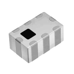
Espinoza recently spoke about some of the activity taking place within his group. “The main part of our communication products group is represented by all our components for RF applications—our LTCC-based and thin-film-based products,” he says. “These products include our filters, diplexers, triplexers, baluns, and couplers (Fig. 2).”
2. Among TDK’s selection of RF components is the TPX Series triplexers, which measure 2.0 × 1.25 × 0.9 mm.
Specific products include the DEA and TFS Series filters, as well as the DPX Series diplexers and the TPX Series triplexers. TDK also offers baluns such as the HHM1 and TFS Series. And the company’s circulators and isolators are key components for small-cell applications.
Another major focus is antennas. Espinoza notes that TDK now offers an online antenna design tool. “We have a tool online right now,” he says. “Let’s say you’re designing a product that uses a standard 2.4- or 5-GHz antenna. You have small chip antennas with very small keep-out areas. But changing that keep-out area is going to affect antenna efficiency and voltage standing wave ratio (VSWR).
“We have a tool online that lets you vary the keep-out area and see how that’s going to impact performance. Designers can use this tool to optimize their boards. There are some external components that are used for matching, and we actually recommend the value of them based on the keep-out area size on the printed-circuit-board (PCB).”
Surmounting Today’s Challenges
There’s no question that today’s requirements have created additional challenges in the RF world. For instance, there’s the ever-present demand for smaller products. According to Espinoza, TDK is helping to meet these small-size requirements. “We’re working with RF front-end module makers. These companies are asking us for very low-profile components. For this, we’re utilizing many of our thin-film solutions. We offer a variety of thin-film products that can be used in module-type applications. Many of these components are size 0605, or even smaller.”
Espinoza believes that issues surrounding PCB layouts represent another common theme due to today’s higher densities. “The other area we’re getting into is layouts,” he adds. “Layouts in RF were always important. But when you didn’t have a high density of components on a PCB, you had a little bit more leeway in terms of how you could execute board layouts.”
Today, higher densities have created additional challenges. Espinoza notes, “Now, as everything is getting closer and closer, we’re starting to see a lot more issues with ground layers—people are using ground structures that are different than what we recommend on our datasheets. They’re putting a lot more via holes in different locations. So, with more integration, the result is often a little bit of shifting in the performance of a product. The attenuation poles tend to shift up when you change some of the ground structures.”
Shielding is a significant factor, too. Espinoza uses the case of a diplexer as an example. “Most diplexers have the inductors in the top layers of the structure,” he says. “If the diplexer is too close to or right below a metal shield, the diplexer could detune a little bit—the attenuation poles could shift up. What we’re doing is providing shielded diplexers. These are internally shielded, and you can just lay them out on a design and not have to worry so much about where it’s going to be used. Another issue is that if you put a diplexer right next to a very noisy inductor, there will be coupling into the diplexer. Using a shielded diplexer will mitigate that effect.”


