Bandpass Filters Feature Wide Tuning Ranges
Download this article as a .PDF
Classical LC filter design is becoming increasingly rare in much of the RF design community. This is in part due to the domination of direct-conversion in up- and down-converters along with the widespread availability of excellent off-the-shelf filter components, such as surface-acoustic-wave (SAW) filters. However, tunable bandpass filters are still required for many applications, whether for discrete designs or on-chip integrated-circuit (IC) designs. If insertion loss must be as low as possible, a peaked-response lowpass filter may be used in order to side-step the higher insertion loss of a true bandpass filter. If attenuation is required in both stopband regions, however, a bandpass filter is generally required.
Bandpass filters (BPFs) have an inherently higher insertion loss than lowpass filters (LPFs) given similar design requirements. A first-order BPF can be designed for low passband insertion loss, but it will suffer from poor stopband attenuation roll-off and rounded passband shape. A second-order BPF can be designed to have appreciably faster stopband transition regions and a reasonably flat passband shape, but normally exhibits higher passband insertion loss than the first-order filter. Only the second-order filter design case will be considered here, whereas extensive details for the first-order filter design can be found in ref. 8.
Filter Design Preliminaries
The author learned a great deal early in his engineering career from the book by Daniels.1 It provided an early appreciation for filter pole/zero placement and was the primary motivation for thinking about the second-order filter design problem in the context of Table 1.
Good control of the internal impedance levels within a lumped-element LC filter is crucial for obtaining reasonable component values and keeping stray inductance and stray capacitance issues at bay. A filter’s internal resistance level can be crafted in a fairly flexible manner in order to realize a range of filter bandwidth versus center frequency behaviors. Choosing series LC-resonators versus parallel LC-resonators is largely determined via the means by which the filter’s center frequency is to be tuned—such as by varactor diodes, FET switches, PIN diodes, or microelectromechanical-systems (MEMS) devices—and having reasonable component values.
Parallel resonators are usually more advantageous for lower insertion loss since these are typically used with an internal filter impedance, Rinternal, which is greater than the port impedances, Rsource and Rload.
In order to make a filter tunable, its inductors and/or capacitors must be tunable. Since tunable inductors are rather intractable for traditional LC filters, the tuning elements are usually limited to capacitors. Since inductors also tend to be more lossy and larger than capacitors, it is desirable to minimize the number of inductors used—nothing new here.
Pole and zero placement for a filter determine all of the behavior characteristics of the filter. It is generally desirable to have an equal number of transmission zeros at dc and infinity so that the lower and upper stopband behaviors can be made roughly symmetric. A representative filter to aid in this discussion is shown in Fig. 1. In order to determine the number of transmission zeros at dc in Fig. 1, it is helpful to think of each capacitor being replaced by an open-circuit and each inductor being replaced by a short circuit, as shown in Fig. 2. In the portion denoted as Cut 1, in a resistive divider sense, an impedance open (from C2) is working against an impedance short (from L1), thereby contributing two transmission zeros (see footnote).
In the portion denoted as Cut 2, an impedance open (from C3) is working against a non-zero impedance Rload, thus adding only one transmission zero. The filter consequently has three transmission zeros at dc.
In the case of transmission zeros at infinite frequency, each capacitor is replaced by a short circuit and each inductor is replaced by an open circuit, as shown in Fig. 3. For Cut 3, a short (from C1) is working against a non-zero impedance, Rsource, thereby contributing one transmission zero. For Cut 4, an open circuit (from L2) is working against a short circuit (from C4), thereby contributing two transmission zeros. The filter consequently exhibits three transmission zeros at infinite frequency, making for an equal number of transmission zeros in the lower and upper stopbands as desired.
Of the second-order filter topology configurations shown in Table 1, having roughly equal numbers of transmission zeros at dc and infinite frequency helps assure good overall stopband performance as just explained. This criterion favors Configurations 2 and 4. Both topologies use parallel resonators, so that is not a discriminating factor. Configuration 2 is the more interesting of the two, however, because it permits Rinternal to be larger than the port impedances, whereas Configuration 4 is just the opposite. The design details behind both configurations will be presented shortly.
This type of tunable second-order BPF was earlier used in connection with an SBIR project.2 Two circuit sketches from that report that make use of this filter type are shown in Figs. 4 and 5. Both make use of inductive-coupling between the two resonators based upon the tee-to-pi transformation. Note that inductive impedance transformations were used at the input and output of the filter, rather than capacitive transformers as used in Configuration 2 of Table 1.
The notion of admittance and impedance inverters is not new.3, 4, 5 They were used in ref. 2 as the basis for Figs. 4 and 5.
Table 2 shows the filter topologies which are the focus for the remainder of this article. Two related topologies can be created by making use of the pi-to-tee network transformation for the inductor sections. The design of Configuration I in Table 2 begins by defining the following initial design parameters
flow = Minimum tunable filter center frequency (Hz);
fhigh = Maximum tunable filter center frequency (Hz);
Bgeo = −3 dB RF filter bandwidth (in Hz) at the geometric center frequency;
Rgeo = Internal filter impedance (in Ω) at the geometric center frequency of the filter;
Ro = Port impedance, usually taken as 50 Ω;
γ = Constant value. A value of γ = 1.0 results in a constant-Q filter design, while a value of γ = 2.0 results in a constant-bandwidth filter design. A value between one and two will yield a blend of the two filter characteristics. Inductor Q values will be more critical as the value of γ is increased.
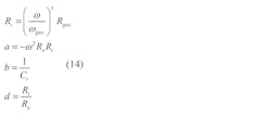
The internal impedance level of the filter is represented by Rt, and is given by
Rt = Rgeo(ω/ωgeo)γ
It is important to note that Rt should always be greater than the port impedance, Ro, at the band edges of the filter.
The geometric center frequency of the filter, ωgeo, is given by
while the coupling inductor, Lc, is given by
and the total tuning capacitance at the geometric center frequency is as follows
Since the inductance values in the filter are fixed, the total tuning capacitance versus the center frequency is given by
Tuning capacitances C1 and C2 are given by Eqs. 7 and 8
The design for Configuration II begins with the same initial parameters as given for the first configuration. The design formulas are a bit more involved for this configuration. The coupling inductor value, Lc, is given by
with
Continuing
Next, define the following quantities
and then compute α and β as follows
The solution for capacitance C1 can be found by solving the quadratic equation
from which C2 follows as
All of the capacitance values can be physically realized using varactor diodes and are therefore tunable. This makes it possible to tune the filter center frequency and adjust the port impedances as desired.
Filter Prototypes
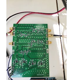
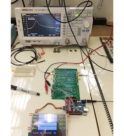
Using these design methods, filter prototypes were built and characterized that covered 10 MHz through 640 MHz (Figs. 6 and 7). Since each tunable filter requires as many as four individual tuning voltages, an Arduino Uno was used to create the four voltages that were then heavily filtered and scaled with the op-amp circuitry in the lower half of Fig. 6. This approach simplified the amount of test equipment needed while making direct-reads of the tuning voltages very convenient. Figure 8 shows a spectrum analyzer measurement using this arrangement.
For interested readers, the original work papers in refs. 8-10 are available in their entirety (102 pages) upon request. The original materials include exhaustive design formula derivations, complete schematic details, additional characterization results, and a helpful filter design MATLAB script.
AM1 LLC, 36068 Hidden Springs Rd., Ste. C-134, Wildomar, CA 92595
Footnote
Note that parallel open circuits count as simply one open circuit, while parallel short circuits count as a single short circuit. The converse is true with series open and short circuits.
References
- Richard W. Daniels, Approximation Methods for Electronic Filter Design, McGraw-Hill, New York, 1974.
- A. Crawford, “Advanced Manpack Radio Concept for UHF DAMA Satellite Communications,” SBIR AF91-030, March 1992.
- George L. Matthaei, Leo Young, and E.M.T. Jones, Microwave Filters, Impedance-Matching Networks, and Coupling Structures, Artech House, Norwood, MA, 1980.
- Gabor C. Temes and Sanjit K. Mitra, Modern Filter Theory and Design, Wiley, Hoboken, NJ, 1973.
- Alan Davis, Microwave Semiconductor Circuit Design, Van Nostrand Reinhold, Philadelphia, 1984.
- A.G. Malherbe, Microwave Transmission Line Filters, Artech House, Norwood, MA, 1979.
- Peter A. Rizzi, Microwave Engineering Passive Circuits, Prentice-Hall, Upper Saddle River, NJ, 1988.
- A. Crawford, “Versatile Bandpass Filters with Wide Frequency Tunability- Part I,” Version 2.01, 2017.
- A. Crawford, “Versatile Bandpass Filters with Wide Frequency Tunability- Part II,” Version 1.0, 2017.
- J.A. Crawford, “Versatile Bandpass Filters with Wide Frequency Tunability- Part III,” Version 1.0, 2017.


