Additive Manufacturing Yields Optimized Antennas
Download this article as a .PDF
Antennas are electronic components that rely on precise mechanical engineering for performance. As communications and other electronic systems grow in complexity, so too do the antennas required to transmit and receive their waveforms. But through the use of additive manufacturing (AM) and three-dimensional (3D) metal printing, even advanced antenna arrays can be reduced in size and complexity. By redesigning a Ka-band 4 × 4 monopulse array and producing it with a 3D printer, what had been a complex component with 100 different parts was reduced to a smaller, single-piece antenna with the same performance capabilities.
The reduction of size and number of parts wasn’t the only benefit gained by 3D printing the antenna array. Conventional methods of manufacturing antennas such as this monopulse array can take eight months of development time on average, plus three to six more of build time. By using 3D printing for this monopulse array test case, it was possible to reduce the lead time to two months. In addition, production costs were reduced by 20 to 25% and nonrecurring-engineering (NRE) costs reduced by 75%. The savings in the weight of the monpulse array amounted to an almost unbelievable 95%.
In addition to what this test-piece project revealed about its capabilities, 3D printing was also found to offer a number of other advantages. When designing multiple antenna components into a single part, the result is an overall reduction in the insertion loss of the combined parts. Because antennas produced by means of AM and 3D laser printing are so much smaller than antennas produced by conventional subtractive manufacturing methods, this also lowers insertion loss dramatically despite the higher surface roughness of the AM construction, for similar or even better RF performance than conventional assemblies.
The 3D metal printing process can be performed with a number of different metals, including titanium and stainless steel, but aluminum is the preferred building material for antennas. This is due to its high surface conductivity and strength when exposed to shock and vibration. It’s also lightweight with strong corrosion resistance.
In terms of RF performance, metal produced by means of 3D metal printing exhibit virtually the same properties as a solid piece of the same material. Metal structures produced by 3D laser printers have been tested in rigorous vibration environments and exhibit the same coefficient of thermal expansion (CTE) as wrought metals. This also gives them better stability over temperature than plastic RF components.
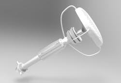
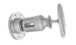
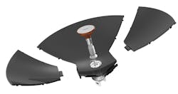
AM allows a new way of manufacturing antennas, although the use of AM also requires antennas to be designed for 3D printing. Early adopters of 3D printing applied it to the creation of prototypes, but antennas designed with industrial AM production in mind can be produced quickly and with less complexity than traditional subtractive manufacturing methods, in which unnecessary materials are removed to leave behind the desired structures (Fig. 1). The Ka-band monopulse tracking array is one example of what is possible by applying AM to the design and production manufacturing of RF/microwave antennas (Figs. 2 and 3).
Optimum use of AM for component design depends on a seamless interweaving of design and 3D printing to precisely meet customer specifications. Often parts that were originally intended to be produced by means of traditional subtractive manufacturing methods do not take full advantage of the benefits of 3D printing.
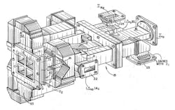
In fact, conventional manufacturing methods can negatively impact RF performance (Fig. 4). Those problems add time and money to traditional antenna manufacturing, as there are often a huge number of parts in a conventional design: typically a daunting array of 100 or more individual metal components—including the hollow, rectangular waveguides so critical for channeling the electromagnetic energy carrying the data—that are joined together via brazing, plunge electrodeposited metal (EDM), and/or multiple bolted joints.
Such assemblies can be large, with unique shapes creating internal geometric hazards that can interfere with the flow of the very data the antenna is supposed to convey. The joining of the different parts has the potential to form a discontinuity that can cause RF losses and reflections. Even the tightness of the screws used to join parts can cause variations in the insertion loss performance. Each of the seams can turn into an unwanted smaller “subantenna” of the main structure.
Tolerances can also be an issue when a hundred or more parts are joined together (Fig. 5). Each of the many separate parts must be inspected independently, then assembled with the hope that their sum will translate into the expected RF performance. The tolerances of each part must be precise; however, when many pieces are integrated together, the tolerance stackup can become significant, resulting in electrical performance degradation.
In contrast, AM and 3D printing support a more precise type of systems-engineering approach. By viewing an antenna assembly as an integrated structure in which all the parts are combined into a single functional part, it is possible to reduce lead times on new antenna designs from months to weeks; dramatically reduce the size and weight of the antenna; and offer resulting cost benefits to customers. Of course, refining any 3D printing process for RF design requires extensive testing to validate that performance meets expectations.
The use of 3D AM to produce antennas results in components that are routinely smaller than antennas built with conventional manufacturing approaches. The smaller size of their additively manufactured products greatly shortens the overall distance that an RF signal had to travel within the system—a huge benefit to antenna performance. The accuracy and precision afforded by AM methods supports the mechanical tolerances and dimensions needed for higher-frequency microwave and millimeter-wave antennas—such as those used in satellite communications, line-of-sight (LOS) communications, aircraft systems, and unmanned aerial vehicles (UAVs)—with the small sizes and light weights of the antennas providing added benefits for these applications.
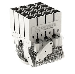
The Ka-band monopulse tracking array produced as a one-piece component (Fig. 6) was characterized at frequencies to 30 GHz, both for benchtop and outdoor environments. Similar designs have passed demanding vibration testing for military requirements. Other antennas designed and produced by means of 3D AM have achieved operating frequencies as high as 50 GHz.
The 3D laser printer from Concept Laser (see below) used to manufacture antennas provides fine mechanical resolution with smooth metal surfaces. Aluminum is the material of preference for a build; it stands up better than plastics to environmental stresses (from terrestrial applications to outer space), and has essentially the same properties as a solid piece of the same material.
The antennas are designed specifically for the AM process. A design starts with the RF requirements for the finished product. The use of AM is coupled with RF/microwave design expertise to avoid internal geometry issues, as well as to deliver the lowest insertion loss and the highest RF possible for each design. Passing inspection can be challenging, since many critical geometries are internal and formed by laser melting—rather than achieved by assembling separate parts—and can’t be measured directly.
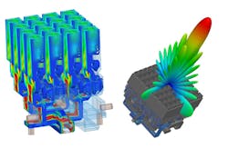
To create an antenna with AM 3D printing, a microwave simulation of the antenna design has been developed using ANSYS HFSS 3D electromagnetic (EM) simulation software from ANSYS. The software models the high-frequency EM field inside the air cavity of the proposed antenna array (Fig. 7). Once a satisfactory HFSS simulation has been developed, the file is imported into SolidWorks 3D CAD software from SolidWorks to determine the optimum thickness for the aluminum walls that will surround the array’s air cavity and enable 3D printing the design as a single metal assembly.
An optimum topology is developed, adding just enough extra material where needed to create an integrated unit that will print consistently. Support structures are also added where needed, using Autodesk Within 3D printing software from Autodesk and merging the result using SolidWorks and software from Magic Software. In this manner of designing and producing an RF antenna, an antenna can be created and modified according to any number of specialized requirements. These include thermal, stress, structural, and tolerance analysis, along with system-level electrical requirements for the antenna.
AM simplifies the addition of new features to an existing 3D design, as well as the assembly of finished parts—except, of course, in those cases where a design is produced as a single part, where no assembly is required. Over time, the AM 3D printing approach can allow for further reduction in an antenna’s parts count, refining the design for smaller size and improved performance. As the number of parts decreases, the amount of rework diminishes and production time declines. As an added benefit, antennas and other components with fewer parts require less maintenance and service over time.
3D Metal Printing Technology At a Glance
Antennas, waveguide components, and other metal parts at Optisys are manufactured with a 3D metal printing system from Concept Laser, a GE Additive company. It uses a high-energy laser to melt and fuse standard commercial batch materials in powdered form. A single-component metal powder is first completely fused. Once it has set and solidified, it is a finished component with almost ideal material properties. Precise contours can be formed by using a scanner. A 3D component is constructed layer by layer, applying and melting additional metal powder as needed. Layer thicknesses can be controlled from 15 to 500 μm.
Parts are created without mechanical tools, without the limits of conventional subtractive manufacturing methods on component geometries or internal configurations, drawing upon input data from 3D electromagnetic (EM) simulation and computer-aided-design (CAD) software. The 3D laser printer produces parts without waste, in contrast to the etching and cutting of conventional metal manufacturing processes. The LaserCUSING laser-based metal melting process does not produce emissions, forming 3D structures with high efficiency.
Clinton Cathey, Chief Executive Officer, and Rob Smith, Chief Operating Officer
Optisys, 6764 Airport Rd., West Jordan, UT 84084; (801) 664-5595
