Dual-Band Bandpass Filter Has Tunable Passband Frequencies
Download this article as a .PDF
Dual-band bandpass filters (BPFs) provide the functionality of two separate filters, but in the size of a single filter. They have become an important part of many multiple-band communications systems, passing desired channels while rejecting unwanted interference and noise.
By using a pair of quarter-wave (λ/4) uniform-impedance resonators (UIRs) and a pair of λ/4 stepped-impedance resonators (SIRs), it was possible to construct a dual-band BPF with center frequencies of 1.57 and 2.07 GHz and fractional bandwidths (FBWs) of 4.46% and 4.35%, respectively. The filter, with tunable center frequencies, provides good selectivity and high out-of-band suppression, using folded resonators for extremely compact size.
A number of methods have been developed for the design of dual-band BPFs.1-8 They can be designed by using two dissimilar BPFs in parallel or cascade with common input/output (I/O) coupling structure. While this technique makes it possible to adjust the passband frequencies independently, it leads to a filter with relatively large size.1 In ref. 1, a dual-band BPF employing a short-circuited λ/4 resonator and an improved SIR was presented, using a split-ring scheme to achieve small circuit size. In ref. 2, a dual-band filter was designed with λ/4 resonators. In this approach two separate passbands were created from one initially wide passband by forming a stopband between the two bands.
Dual-mode resonators are widely used in dual-band BPFs.3, 4 In ref. 3, two dual-mode cross-slotted patch resonators are arranged back-to-back to design a multilayer dual-band BPF. The passband frequencies can be controlled separately. Reference 4 synthesizes a dual-band BPF with two identical SIRs, obtaining good selectivity in the process. However, this filter’s passband frequencies are not independent and the filter circuit is relatively large.
Another popular way to design dual-band BPFs is by employing multimode resonators.5-7 This approach leads to a dual-band BPF with small size, but with limited independent tuning of the passband frequencies due to the internal structure of the filter.
In ref. 5, a dual-band BPF was designed with a novel quad-mode resonator using coupled line sections and transmission-line section. This design offers good selectivity and small size. In refs. 6 and 7, dual-band BPFs using multiple stub-loaded ring resonators and filters based on E-shaped multimode resonators were presented, respectively. The resonant modes of these two resonators can be individually controlled. Reference 8 presents a dual-band BPF using symmetric double-spiral resonators. The filter has small circuit size, but is difficult to synthesize.
As an improved approach to implementing a dual-band BPF with independently controlled passband frequencies, a filter was developed with center frequencies of 1.57 and 2.07 GHz using two λ/4 UIRs and two λ/4 SIRs. The FBWs of the two passbands are 4.46% and 4.35%, respectively. Figure 1 illustrates the filter’s structure. Not only are the folded resonators embedded together, but the coupling lines are placed between the resonators to create a layout with small size.
The filter was analyzed by deducing the input admittance of the resonators. Both passband frequencies can be tuned independently by changing the dimensions of each resonator. Furthermore, source-load coupling is applied to generate two transmission zeros at the passband edge, leading to good selectivity and an improved stopband up to 4.74 GHz (2.3f2).
Figure 1 shows the layout of a second-order dual-band BPF developed with this new approach. It consists of two folded λ/4 UIRs and two folded λ/4 SIRs. The UIRs and SIRs are embedded together and the coupling lines are placed between the resonators, which makes the filter very compact. The λ/4 UIRs generate the first passband while the λ/4 SIRs form the second passband. Two additional coupling lines realize source-load coupling.
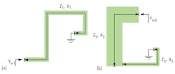
Figures 2a and b present schematic diagrams of the λ/4 UIR and λ/4 SIR. The input admittances of the UIR and SIR are derived by Eqs. 1 and 2:
Yin1 = jcotθ1/Z1 (1)
Yin2 = (Z2 – Z3tanθ2tanθ3)/[jZ2(Z2tanθ2 + Z3tanθ3)] (2)
where Z1 and θ1 denote the UIR’s impedance and electrical length, respectively, at frequency f1. Parameters Z2 and Z3 are the impedances of the SIR while θ2 and θ3 indicate the electrical lengths at f2. Frequencies f1 and f2 are the center frequencies of the first and second passbands, respectively. The conditions of resonance can be deduced by Eqs. 3 and 4 when Yin1 = 0 and Yin2 = 0:
θ1 = π/2 at f = f1 (3)
Z2 = Z3tanθ2tanθ3 = 0 at f = f2 (4)
The dimensions of the resonators can be derived once the passband frequencies are defined. The electrical length θ1 is determined by the various structural parameters, including L1, L2, L3, L4, and L5, which determines the value of f1. It is convenient to adjust f1 by tuning the value of L5 without having much influence on the coupling coefficients.
As for tuning the value of f2, both the impedance ratio of Z2/Z3 and the electrical lengths θ2 and θ3 can be used for adjustment. W2 and W3 determine Z2 and Z3, while θ2 and θ3 are decided by L6, L7, L8, L9, and L10. Likewise, W3 and L10 are used to adjust f2 with minimal effect on the coupling coefficients of the whole structure.
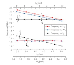
Figure 3 plots the center frequencies of both passbands with different values of L5, L10, and W3. The variation of L5 changes f1 distinctly and f2 keeps constant. On the other side, f2 can be adjusted by tuning L10 and W3, while f1 has nearly no change. This demonstrates that f1 and f2 are independently controllable.
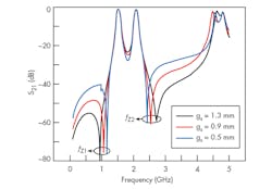
Figure 4 shows that two transmission zeros are generated. These two transmission zeros are created because of the source-load coupling introduced by the two additional coupling lines. One transmission zero is located below f1 while the other is above f2. Both transmission zeros are very close to the passbands, effectively improving the filter’s selectivity. The filter also exhibits good high-frequency signal suppression due to the transmission zero above f2.
The locations of both transmission zeros can be controlled by changing gs. As depicted in Fig. 4, both transmission zeros can be moved closer to the passbands by reducing gs. The band-to-band isolation will be slightly improved in the process, although some degradation of the high-frequency signal suppression will occur as an unwanted side effect. Thus, the locations of the transmission zeros must be weighed carefully according to the specific design requirements of an application.
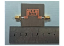
To demonstrate the effectiveness of this design approach, a dual-band BPF centered at 1.57 and 2.07 GHz was designed and fabricated on Arlon DiClad 880 substrate (the company is now part of Rogers Corp.) with dielectric constant of 2.2, substrate thickness of 0.762 mm, and conductor thickness of 0.035 mm. The fabricated dual-band BPF is illustrated in Fig. 5.
All detailed geometry dimensions of the filter are given as follows (in mm): g1 = 0.3 mm, g2 = 0.3 mm, g3 = 0.9 mm, g4 = 0.2 mm, g5 = 0.2 mm, g6 = 0.5 mm, L1 = 2.1 mm, L2 = 4.1 mm , L3 = 8.4 mm, L4 = 11 mm, L5 = 5 mm, L6 = 0.3 mm, L7 = 1.7 mm, L8 = 5.1 mm, L9 = 6 mm, L10 = 2.5 mm, L11 = 7.8 mm, L12 = 1.8 mm, L13 = 4.35 mm, L14 = 9.15 mm, L5 = 11.45 mm, W1 = 1.2 mm, W2 = 0.6 mm, W3 = 2.5 mm, W4 = 2 mm, W5 = 1 mm, W6 = 0.3 mm, W7 = 2.3 mm, and D1 =0.4 mm.
Not including the two feed ports, the filter circuit measures about 0.1λg × 0.24λg (13.75 × 31.9 mm), where λg indicates the guided wavelength at f1 = 1.57 GHz. Both UIRs and SIRs are folded and embedded together to achieve compact circuit size. Two additional microstrip lines are linked to the main coupling lines to achieve source-load coupling.
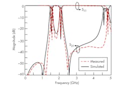
A model N5245A vector network analyzer (VNA) from Keysight Technologies was used to measure the performance of the fabricated dual-band BPF. Figure 6 plots the simulated and measured frequency responses, which are in close agreement. It can be seen that two passbands are centered at 1.57 and 2.07 GHz with FBWs of 4.46% and 4.35%, respectively.
The measured results indicate that the insertion loss (IL) is 1.54 and 1.68 dB at the first and second passbands, respectively. The return loss (RL) is better than 24 dB within the two passbands and the band-to-band isolation is greater than 20 dB from 1.68 to 1.94 GHz.
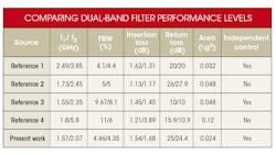
In addition, two transmission zeros were created at fZ1 = 1.22 GHz and fZ2 = 2.48 GHz, which improve the selectivity of both passbands. The filter shows good high-frequency signal suppression of greater than 20 dB to 4.74 GHz (2.3f2). The table offers a comparison between the proposed filter with some other reported dual-band BPFs. It demonstrates that this filter realizes both compact size and independently controllable passband frequencies at the same time.
This combination of folded λ/4 UIRs and folded λ/4 SIRs and an embedded structure for small size represents an effective approach for designing a dual-band BPF with independently controllable passbands. The passband insertion loss is low and the output-of-band suppression is high, making this design a suitable candidate for many communications applications with multiple channels.
Lamin Khan, Associate Professor
Pei Qiu, Master’s Degree Candidate
School of Optical and Electronic Information, Huazhong University of Science and Technology, Wuhan 430074, China
Baoquan Hu, Engineer
Changzhong Chen, Engineer
Avic Shaanxi Aircraft Industry (Group) Corp. Ltd., Xi’an Shaanxi, China
Acknowledgment
This work was supported by the National Natural Science Foundation of China, under grant No. 61001012.
References
1. G. Wu, L. Yang, and Q. Xu, “Miniaturized dual-band filter with high selectivity using split ring scheme,” Electronics Letters, Vol. 51, No.7, April 2015, pp. 570-572.
2. S. Zhang and L. Zhu, “Compact Split-Type Dual-Band Bandpass Filter Based on λ/4 Resonators,” IEEE Microwave and Wireless Components Letters, Vol. 23, No. 7, July 2013, pp. 344-346.
3. G. Zhang, J. Chen, J. Shi, H. Tang, H. Chu, and Z. Bao, “Design of Multilayer Balun Filter With Independently Controllable Dual Passbands,” IEEE Microwave and Wireless Components Letters, Vol. 25, No.1, January 2015, pp. 10-12.
4. Z. Songbai and Z. Lei, “Fully canonical dual-band bandpass filter with λ/4 stepped impedance resonators,” Electronics Letters, Vol. 50, No.3, January 2014, pp. 192-194.
5. Y. Peng, L. Zhang, J. Fu, Y. Wang, and Y. Leng, “Compact Dual-band Bandpass Filter Using Coupled Lines Multimode Resonator,” IEEE Microwave and Wireless Components Letters, Vol. 25, No.4, April 2015, pp. 235-237.
6. J. Xu, W. Wu, and G. Wei, “Compact Multi-Band Bandpass Filters With Mixed Electric and Magnetic Coupling Using Multiple-Mode Resonator,” IEEE Transactions on Microwave Theory & Techniques, Vol. 63, No.12, December 2015, pp. 3,909-3,919.
7. H.W. Liu, S. Li, and B.P. Ren, “Microstrip dual-band bandpass filter with E-shaped multimode resonator,” Electronics Letters, Vol. 49, No.14, July 2013, pp. 887-888.
8. G. Wu, G. Wang, J.G. Liang, X. Gao, and L. Zhu, “Miniaturized microstrip dual-band bandpass filter using novel symmetric double-spiral resonators for WLAN application,” Electronics Letters, Vol. 51, No. 15, July 2015, pp. 1,177-1,178.


