Efficient GaN Doherty Amplifier Peaks at 1 kW from 2.11 to 2.17 GHz
Download this article in PDF format.
Power amplifiers are among the most important of components for modern wireless communications systems. Ideally, they can provide high output power with high linearity and high efficiency. But tradeoffs typically occur among these three key power-amplifier performance parameters, and amplifiers with the highest output power and linearity usually sacrifice linearity.
In modern telecommunications systems supporting wide bandwidths and high data rates, transmitted signals are usually characterized by high peak-to-average power ratio (PAR) due to wide and rapid variations in the instantaneous transmitting power. Therefore, it is a challenge to design a wireless base-station power amplifier having high efficiency not only at maximum output power, but at lower power levels typically ranging from 6 dB and less of the maximum power level, with minimum size and lower cost of implementation.
However, the problem is solvable by using gallium-nitride (GaN) high-electron-mobility-transistor (HEMT) device technology and innovative Doherty amplifier architectures. It’s possible to achieve 60% average efficiency and reduced power consumption for average output-power levels of 100 W and higher.
Getting on Board with GaN HEMTs
GaN HEMTs feature high breakdown voltages, high current densities, high transition frequency (fT), low on-state resistance, and low parasitic capacitance, resulting in a wide-bandwidth amplifier featuring high-power capabilities and high operating efficiency. The high power density enables physically compact designs, while high dc-supply-voltage operation and low parasitic output capacitance lead to higher load impedance for ease in obtaining wide impedance bandwidths. In addition, the high drain-to-source breakdown voltage in excess of 150 V enables rugged operation at 50 V dc regardless of drive level or harmonic load environment.
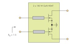
1. This simple schematic rendering represents a dual-path GaN HEMT with internal input impedance matching.
As an example, Sumitomo’s GaN HEMT technology delivers high-gain packaged devices capable of peak output power levels to 300 W at frequencies to 8 GHz and higher. Applications include radar and high-reliability cellular communications transmitters. Progress in increasing power density has resulted in devices with 5-W/mm power density, and as much as 10-W/mm power density at 50 V dc. The use of high-thermal-conductivity substrates such as silicon carbide (SiC) provide excellent thermal stability even at these high power densities.
To achieve high efficiency under backed-off operating power conditions, enhancements such as envelope tracking and outphasing techniques, among others, are available. However, the use of a Doherty amplifier configuration provides a practical alternative approach. A Doherty amplifier is simple to implement and can provide high efficiency across a wide bandwidth when operating with backed-off power, depending on the number of stages. In this case, a three-way asymmetric Doherty configuration offers a suitable compromise among high gain, high output power, and high average efficiency.
GaN HEMTs can be fabricated with larger gate peripheries for higher power capabilities from a given package size. The corresponding increase in gate-source capacitance when multiple device cells are connected in parallel reduces the optimum input impedance to very low values—close to a few tenths of an ohm. As a result, a low-loss matching network is required inside the package to transform the impedance from the reference plane defined by the package leads to the reference plane of the device die.
For practical use, a packaged power device should provide reasonably high (not less than 1 Ω) input impedance with a sufficiently low quality factor (Q) to provide flat gain/amplitude performance over a required frequency bandwidth. Depending on the space within the package, as a simple matching network for narrowband operation (for example, from 2.11 to 2.17 GHz, corresponding to cellular radio band 1), a quarter-wave microstrip line on a high-permittivity substrate might be considered (Fig. 1) for a dual-path package. Here, two separate 180-W GaN HEMT dies are attached in parallel.
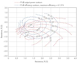
The load pulling of an amplifying path (including the packaging parameters for the transistors), where two 50-V 180‑W transistor die are connected in parallel and biased in a Class AB mode, resulted in the contours of Figure 2. It demonstrates the tradeoff in determining an optimum output impedance match, because the optimum impedance for maximum power is quite different than the optimum impedance for maximum efficiency. In this case, the output power at 1-dB gain compression reaches a maximum of about +55 dBm under low-impedance conditions of (1.2 – j1.1) Ω, whereas a maximum efficiency of greater than 61% is obtained for a purely resistive impedance of about 1.3 Ω (Fig. 2).
2. The load-pull contours show impedances for optimum output power and efficiency.
Modified Doherty Configuration
For a high-power amplifier with very low output impedance, the width of the matching microstrip line is very wide compared to its length and the overall size of the matching circuit. The matching circuitry includes an offset line to create an open-circuit condition when the peaking amplifier is turned off, as well as a quarter-wavelength transforming line. As a result, it can easily become large enough whereby it becomes difficult to connect the output of the peaking amplifier directly to the main amplifier signal path.
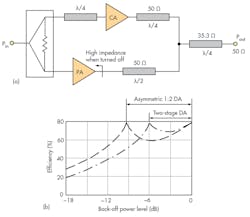
For convenience of implementation, a classical Doherty amplifier configuration can be modified by including an additional one-half-wavelength line at the output of the peaking amplifier. Figure 3a shows the block diagram of a modified two-stage Doherty amplifier configuration, where a one-half-wavelength line is connected to the output of the peaking amplifier (PA) and a quarter-wave line is included at the input of the carrier (or main) amplifier (CA) for phase compensation. This configuration is characterized by the same two peak efficiency points at saturation and where the power is backed off or decreased by 6 dB from its maximum level. It is similar to a classical two-stage Doherty amplifier (DA) as shown in Figure 3b.
3. The block diagram shows a modified symmetric two-stage Doherty amplifier (a) along with its theoretical efficiency (b).
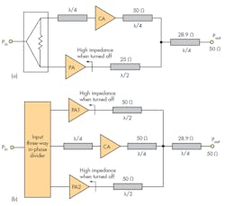
It is possible to extend the region of high efficiency over a wider range of output power levels if the carrier and peaking amplifiers are designed to operate with different output power levels—smaller for the carrier amplifier and larger for the peaking amplifier. For instance, for a power-division ratio 1:2, the transition point with maximum drain efficiency corresponds to the back-off power level of 9.5 dB from peak output power, as shown in Fig. 3b. In this case, the characteristic impedance of a half-wave line is 25 Ω, which corresponds to the load impedance required for the peaking amplifier. The characteristic impedance of the combining quarter-wave line is 28.9 Ω, as shown in Figure 4a.
When it is difficult to choose the proper power ratio between packaged active devices, it is convenient to use identical power amplifiers in a multi-way Doherty configuration, where one carrier power amplifier is parallel with multiple peaking amplifiers. Thus, a 1:2 asymmetric two-stage Doherty structure can be transformed into a modified three-way asymmetric Doherty configuration (Fig. 4b).
4. This block diagram illustrates a modified 1:2 asymmetric Doherty amplifier.
The modified setup includes one carrier amplifying path and two identical peaking amplifying paths when device sizes for the carrier amplifier and both peaking amplifiers (PA1 and PA2) are equal. The half-wave line in each peaking amplifying path can be split into two quarter-wave lines. Each quarter-wave line has its own characteristic impedance for the corresponding impedance transformation when the required load impedance for the peaking device is sufficiently small.
Three-Way Doherty Amplifier
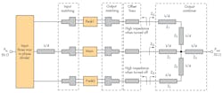
Figure 5 shows the block diagram of a three-way asymmetric Doherty amplifier configuration. The output combiner includes one-quarter-wavelength microstrip line in the carrier signal path, two-quarter-wavelength microstrip lines in each peaking path, and one quarter-wave microstrip combining line. Here, each amplifying path includes a packaged device with the same die size and input and output matching circuits using microstrip lines.
5. Several quarter-wave microstrip lines are built into a three-way inverted Doherty amplifier.
Offset lines are necessary to provide proper open-circuit conditions at their ends for peaking amplifiers when they are turned off. Then, two quarter-wave microstrip lines with different widths are required for the corresponding impedance transformation. They translate the open-circuit condition in each peaking path to the open circuit seen by the carrier path at output-power levels lower than 9 dBc at a common node in the output combiner.
For example, for identical amplifiers having optimum load impedance Z0 = 12 Ω each and Z2 = RL = 50 Ω, where RL is the standard 50-Ω load impedance, Z1 = (Z0Z2)0.5 = 24.5 Ω and Z3 = (Z2RL)0.5/(3)0.5 = 28.9 Ω. There may be different combinations of the characteristic impedances between quarter-wave microstrip lines in the output combiner. The quarter-wave microstrip line in the input path of the carrier amplifier is used to compensate for the delay provided by the output combiner.
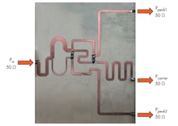
The input three-way in-phase power divider (Fig. 6) was implemented on 20-mil-thick RO4350 circuit material from Rogers Corp., which was also used to implement the entire Doherty amplifier circuit. It includes a transforming quarter-wave line, and an asymmetric 1:2 two-way Wilkinson divider to split power between the two signal paths, one with the carrier and first peaking amplifiers and the other with the second peaking amplifier. Also incorporated is a symmetric two-way Wilkinson divider to equally split power between the carrier and first peaking amplifiers; an additional 50-Ω quarter-wave microstrip line in the carrier path; and three equal-length 50-Ω connecting microstrip lines in the carrier and two peaking paths.
6. This is a photograph of an input three-way in-phase power divider with additional quarter-wave line.
Test Results
The test board of a modified three-way Doherty amplifier based on three dual-path GaN HEMT devices in metal-ceramic flange packages, each including a pair of 180-W GaN HEMT dies with internal input matching, was fabricated on 20-mil-thick RO4350 circuit material. The input three-way divider, input and output matching circuits, offset lines, output combiner, and gate and drain bias circuits (having bypass capacitors on their ends) are fully based on microstrip lines of different electrical lengths and characteristic impedances. Special care was taken for the device implementation process to minimize the output lead inductances of the packaged GaN HEMT devices.
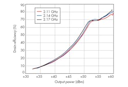
7. The plots show measured drain efficiency as a function of output power.
The output power at 1-dB gain compression point P1dB was measured at 60 dBm, while peak efficiency of 80% and power gain of about 15 dB were achieved at a supply voltage of 55 V dc within a frequency range of 2.11 to 2.17 GHz. Figure 7 shows the plots of the drain efficiency versus output power, revealing a drain efficiency of about 70% at around 8.5-dB power back-off.
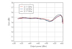
For a 20-MHz Long Term Evolution (LTE) signal with 8-dB PAR, an average power of 52 dBm was obtained with a drain efficiency of about 65%. In this case, a power gain of about 15 dB was achieved in a linear operating region having 2-dB flatness over the entire output power range to 60 dBm when its value is reduced by just 1 dB compared to its value in the linear region (Fig. 8).
8. Here, the plots reveal measured gain as a function of output power.
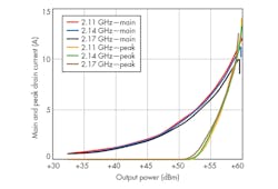
Figure 9 shows the measured dc drain current of the main and peaking amplifiers versus output power. The cutoff point of the peaking amplifiers, when turned off, is about 50 dBm across the operating frequency range of 2.11 to 2.17 GHz.
This is the first implementation of a 1-kW three-way asymmetric Doherty amplifier configuration based on innovative Sumitomo GaN HEMT device technology. It features 65% average drain efficiency for cellular communications transmitters operating from 2.11 to 2.17 GHz.
9. The drain currents for the carrier and peaking amplifiers are plotted as a function of output power.
It was shown that high average efficiency of 65% and high power gain of about 15 dB can be achieved at exceptionally high output power of 1 kW corresponding to 1-dB gain compression point. At the same time, the modified asymmetric Doherty amplifier has the ability to be digitally predistorted to meet stringent spectral mask requirements. This is the highest performance for peak power and drain efficiency ever recorded in a high-power Doherty amplifier development for cellular base-station applications.
James Wong is RF PA Specialist, Naoki Watanabe is Senior RF Engineer, and Andrei Grebennikov is RF PA Specialist for Sumitomo Electric Europe Ltd.

