Analyze Matching Networks For Low-Noise Amplifiers
This file type includes high resolution graphics and schematics when applicable.
Low-noise amplifiers (LNA) set the general noise figure and sensitivity of receivers and other high-frequency systems. Although a variety of excellent low-noise transistors is currently available based on numerous process technologies, achieving good amplifier low-noise performance depends strongly on the required LNA device input impedances and the choice of impedance-matching topologies. By analyzing these choices, it should be possible to find an optimum topology for a given device impedance.
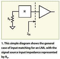
For the example amplifier in Fig. 1, R0 is the signal source impedance (typically 50 Ω), Zin is the amplifier input impedance, and M is a matching network. For simplicity, assume that the matching network is designed for an ideal conjugate (maximum power) match; i.e., it transforms the impedance Zin to the impedance R0. In most cases, the input of an LNA will be matched for minimum noise figure, which may result in a mismatch in terms of power performance. In the case of a lossless matching network, the perfect conjugate match condition implies the following property: if a plane is drawn anywhere within the matching network or at its terminals connected to R0 and Zin, impedances looking in opposite sides of the plane must be conjugate to each other.
For example, impedance looking into the left-hand side of the plane drawn in Fig. 1 must be Zin*. Even if a matching network has loss, it is possible to rearrange its boundaries such that it is purely reactive and all losses are added to either R0 or Zin. So, the property of the conjugate impedances can still be used.
The losses in a matching network are due to the finite quality factors (Qs) of the components used in the matching network. The Qs of surface-mount or even on-chip metal-insulator-metal (MIM) capacitors are usually very high and their contributions to the losses can be neglected. For example, the Q of a typical 2-pF 0402-sized capacitor is about 600 at 1 GHz while the Q of a 10-nH 0402-sized ceramic inductor is only 32 at 1 GHz. From these values, it is apparent that inductors are responsible for most of the losses in a matching circuit. The inductor is also more expensive than a discrete capacitor.
For this analysis of LNA matching networks, all possible LNA input impedance, Zin, will be considered but the number of matching network topologies will be limited to those that:
- contain at most two reactive components, and
- contain at most one inductor.
The assumption that capacitors are lossless implies that a matching network without inductors would also be lossless and need not be analyzed. A matching network with two inductors is assumed to have more loss than a matching network with a single inductor or no inductors.
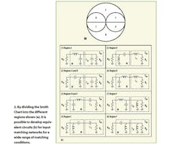
Figure 2a shows how the Smith Chart can be divided into six regions for the purpose of categorizing different matching networks and LNA input impedance, Zin. The input impedance Zin can be presented by a simple equivalent circuit containing a resistor and either a capacitor or inductor. These circuit elements can be connected in either a series or parallel configuration. The analysis is much simpler with the parallel connection when the first matching element on the amplifier side is a shunt element; conversely, the series connection works better when the first matching element on the amplifier side is a series element (both connections can be easily interchanged to represent the same Zin using the Thevenin theorem). Then, all the matching circuits and the analysis cases can be categorized as shown in Fig. 2b. Matching circuits for region E were not analyzed because a series-C/shunt-C matching network should be the obvious choice for this region. For every other region, there are two possible matching networks containing only one inductor. An analysis should show which of the two has lower loss or, equivalently, yields lower noise figure for the LNA.
The main derivations for noise figure require knowledge of the matching inductor value as a function of the matched impedances, which must be derived first. This derivation is simple. First, the impedance looking into the left terminal (from the source side) of a matching network is derived and, then, its imaginary part is forced to be zero and the real part is forced to be equal to R0. The resulting two equations can be solved for the matching capacitor and inductor values. The derivations are omitted here for simplicity but can readily be completed using the MathCAD mathematical analysis software. The results of the derivation for the matching inductor are shown in Eqs. 1 through 6 (indexes 1 through 8 denote the matching inductors from the corresponding matching networks in Fig. 2b):
where:
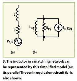
Resistor R models the ohmic losses in the winding conductor of the coil. Parameter Vn,R represents the noise voltage generated by:
It is easy to show that:
where:
Page Title
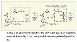
For the purpose of analyzing matching networks 1 and 7, Fig. 4a shows the equivalent circuit of the LNA input where resistor R1 models the ohmic losses in inductor L1. For further derivations, it is convenient to rearrange the equivalent circuit as shown in Fig. 4b so that R1 is outside the boundaries of the matching network.
In this case, the new matching network is lossless and the impedance looking into its left terminal must be (R0+R1) to satisfy the conjugate match condition.
By definition, the noise factor, F, is:
where:
Si and Ni = the powers of the signal and noise, respectively, at the input ofa circuit;
So and No = the powers of the signal and noise, respectively, at the output;
G = the circuit power gain;
Na = the added noise power at the output (in this case, generated by R1); and
NR0 = the output noise power due to the source alone (generated by R0).
The output power is delivered to Zin. Due to the absence of power loss in the rearranged matching network, all input power delivered to its left terminal is exactly the same as the output power delivered to Zin. So, all power calculations can be done at the left terminal as follows:
Parameter R1 can be expressed as L1/QL while L1 can be found from Eq. 1. Then,
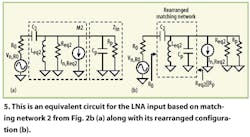
Figure 5a shows the equivalent circuit of the LNA with matching network 2 from Fig. 2b where the shunt matching inductor, L2, is already replaced by its equivalent parallel circuit with Req2 modeling the ohmic losses in L2.
As before, for further derivations, it is convenient to rearrange the equivalent circuit as shown in Fig. 5b so that all reactive elements (including Cp) are lumped together in a new matching network and Req2 is outside of the boundaries of this network, making it lossless. In this case, the new matching network transforms R0 into (Req2||Rp). The output power is delivered to Rp but not (Req2||Rp):
where it is assumed that Req2 >> Rp
(typically, the losses in the matching network shouldn't be allowed to influence the matched impedances). Parameter Req2 can be expressed as:
and L2 can be found from Eq. 2. Then,
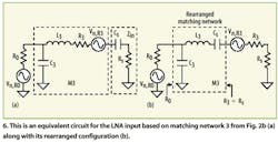
Similar derivations can be performed for the matching network of Eq. 8, resulting in:
The rearranged equivalent circuit is shown in Fig. 6b. The output power is delivered to resistor Rs:
Substitution of R3 = L3/QL and Eq. 3 results in:
Similarly,
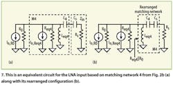
All power calculations can be done at the left terminal of the new matching network:
where Req4 can be expressed as:
and L4 can be found from Eq. 4. Then,
Two matching networks can be used for Zin in region A of the Smith chart (see Fig. 2a): matching networks 1 and 2. Comparison of Eqs. 7 and 8 shows that matching network 1 has a lower noise factor for Qin > 0.
Two matching networks can be used for Zin in region B: matching networks 2 and 3. Comparison of Eqs. 8 and 10 shows that these networks have the same noise figure for Rs/R0 = R0/Rp; i.e., for Zin laying on the vertical line that goes through the center of the Smith chart. To the right side of this line, matching network 3 has a lower noise figure and to the left side of this line, matching network 2 has a lower noise figure.
Two matching networks can be used for Zin in region C: matching networks 3 and 4. Comparison of Eqs. 10 and 12 shows that matching network 4 has a lower noise factor for Qin > 0.
Two matching networks can be used for Zin in region D: 5 and 6. Comparison of Eqs. 11 and 12 shows that matching network 6 has a lower noise factor for Qin > 0.
Two matching networks can be used for Zin in region F: matching networks 7 and 8. Comparison of Eqs. 7 and 9 shows that matching network 8 has a lower noise factor for Qin> 0.
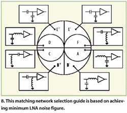
Figure 8 shows the matching network selection guide based on the minimum LNA noise figure.
An LNA designed for PCS-band applications has an input impedance Zin = 42.3-j48.6 at 1.96 GHz. This impedance falls into the region B' (see Fig. 8) where matching networks 2 or 3 can be used. In using the material already covered, it should be possible to calculate the loss of both circuits:
If these inductors are surface-mount ceramic inductors of 0402 case size, their loaded Q, QL, is about 46 at 1.96 GHz. Then:
As shown by the predictions, matching network 3 is preferable.
Depending on where the input impedance of a circuit on the Smith chart, either a series or shunt inductor matching network can be preferred to achieve the lowest loss or, equivalently, NF. The above matching network selection guide can also be used for the output impedances as well (just substitute Zin with Zout).
This file type includes high resolution graphics and schematics when applicable.


