This file type includes high resolution graphics and schematics when applicable.
Circuit traces on microstrip printed circuit boards (PCBs) form the interconnections between components in addition to the components themselves. These controlled-impedance lines are typically designed with a characteristic impedance of 50 Ω for RF/microwave circuits or 75 Ω for cable television (CATV). The equations commonly associated with calculating the geometry of microstrip lines based on a desired impedance are quite complex and not easy to handle. Fortunately, a set of simplified equations has been developed based on well-known publications from IPC (www.ipg.org).
In these simplified equations, the dimensions for thickness, T, must be expressed in microns (m), although the values for height, H, and width, W, can have any measurement unit congruent with one another. The plots shown throughout the article assume a copper thickness of 35 m with the errors are calculated as:
where:
Zcal = the calculated impedance and Ztheor = the expected value (i.e., 50 or 75 Ω
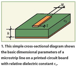
Figure 1 shows a cutaway view of a typical microstrip circuit with the three dimensions and the relative dielectric constant (er). In the IPC's publication IPC-2141, the impedance of a microstrip line is given by:
This relationship can be rearranged to show width, W, explicitly as:
When W is determined for characteristic impedance (Z0 of 50 Ω or 75 Ω the calculations can be performed by means of:
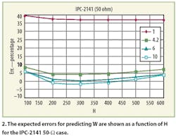
Plots of errors based on circuit-board materials with several different dielectric constants were determined by using the previous equations. The results are shown in Fig. 2.
To simplify the microstrip dimensional formula, the exponential term can be linearized. This linear series expansion leads to:
Assuming a range of dielectric constants (er) from 3 to 10 as in the original formula, the value of x0 = 2.6 for a characteristic impedance (Z0) of 50 Ω and the value of x0 = 5.9 for a characteristic impedance of 75 Ω so that:
Page Title
This can be further simplified to:
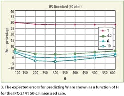
The error curves are shown in Fig. 3 using the linearized relationships and assuming microstrip lines with characteristic impedance of 50 Ω.
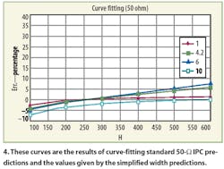
Due to the good results obtained by the linearized formula, the same model was used to fit the values from an EM field solver. This approach led to a surpringly simple equation for the case of a characteristic impedance (Z0) of 50 Ω:
The curves shown in Fig.4 are the result of curve-fitting the error curves that were generated under the same conditions as the original IPC formula and the linearized IPC-based formula.
It is possible to make a further simplification/approximation by disregarding the value of the microstrip line thickness, T:
This last equation confirms the rule of thumb that the ratio of the width to height of a 50 Ω line, W/H, on FR4 circuit-board material, is approximately 2. In fact, for common FR4, the relative dielectric constant (er) is approximately 4.
Shifting to the curve for a characteristic impedance (Z0) of 75 Ω the following equation results:
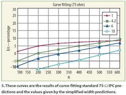
with the same-curve-fitting procedure used to generate the curves shown in Fig. 5.
As in the case with the 50 Ω characteristic impedance, if the microstrip thickness parameter, T, is neglected, the resulting simplified equation is:
These simple solutions can be used for a wide range of RF and microwave microstrip calculations at 50 and 75 Ω.
This file type includes high resolution graphics and schematics when applicable.
About the Author

Leaders relevant to this article:


